

Semiconductor structures and methods of forming them
A technology of semiconductor and protection structure, applied in the direction of semiconductor devices, electrical components, circuits, etc., can solve the problems of NMOS transistor positive bias temperature instability, PMOS transistor negative bias temperature instability and other problems, to reduce the bias voltage Temperature Instability, Reduced Change, Reduced Effect of Drift
- Summary
- Abstract
- Description
- Claims
- Application Information
AI Technical Summary
Problems solved by technology
Method used
Image

Examples
Embodiment Construction
[0034] There are many problems in the method for forming the semiconductor structure, for example, the bias temperature instability of the formed semiconductor structure is serious.
[0035] Combining with a method of forming a semiconductor structure, the reasons for the serious bias temperature instability of the formed semiconductor structure are analyzed:
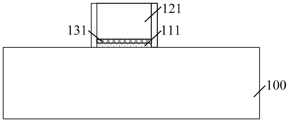
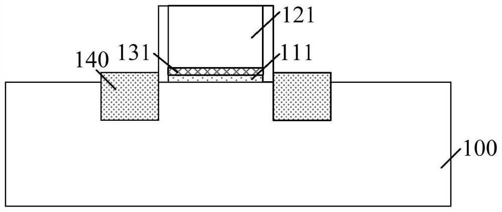
[0036] Figure 1 to Figure 2 It is a structural schematic diagram of each step of a method for forming a semiconductor structure.
[0037] Please refer to figure 1 , providing a substrate 100; forming a gate structure on the substrate 100, the gate structure comprising: a high-k dielectric layer 111 on the substrate 100; the function layer 131 ; the metal gate 121 located on the work function layer 131 .
[0038] Please refer to figure 2 , forming a source-drain doped layer 140 in the substrate 100 on both sides of the gate structure; annealing the source-drain doped layer 140 to activate dopant ions in the source-...
PUM
| Property | Measurement | Unit |
|---|---|---|
| thickness | aaaaa | aaaaa |
| thickness | aaaaa | aaaaa |
| thickness | aaaaa | aaaaa |
Abstract
Description
Claims
Application Information