Method of preparing SOI silicon wafer by adopting rapid heat processing process

A rapid heat treatment, silicon wafer technology, applied in semiconductor/solid-state device manufacturing, electrical components, circuits, etc., can solve the problems of high surface roughness of SOI, uneven temperature of silicon wafers, uneven film thickness, etc.

Active Publication Date: 2019-11-01
SHENYANG SILICON TECH
View PDF4 Cites 0 Cited by
  • Summary
  • Abstract
  • Description
  • Claims
  • Application Information

AI Technical Summary

Problems solved by technology

However, for the process of microwave splitting, the silicon wafer is subjected to uneven temperature, which may easily lead to uneven final film thickness, and at the same time, the surface roughness of SOI after splitting is high.

Method used


Image

  • Method of preparing SOI silicon wafer by adopting rapid heat processing process
  • Method of preparing SOI silicon wafer by adopting rapid heat processing process
  • Method of preparing SOI silicon wafer by adopting rapid heat processing process

Examples


Embodiment 1

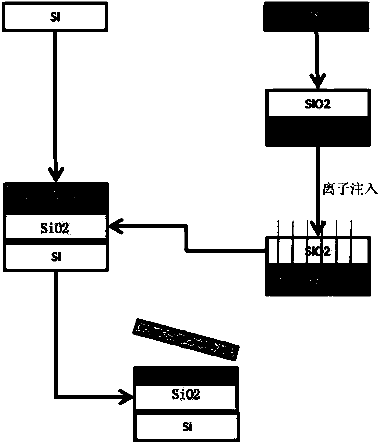
[0025] A method for preparing SOI silicon wafers by using a rapid heat treatment process, which meets the following requirements: it uses silicon wafers as raw materials, and sequentially oxidizes, injects H + and bonding process steps to obtain H + The bonding sheet of the injection layer is split, and then the bonding sheet is cracked by a rapid thermal treatment process (RTP) and a microwave, that is, the desired SOI silicon chip can be obtained.

[0026] The method for preparing SOI silicon wafers using a rapid thermal treatment process meets the following requirements: a rapid thermal treatment process (RTP) single-chip process is used in the splitting process, the temperature is raised to a required temperature not exceeding 480°C, and the temperature is stabilized for 30S-10min. The rate is 10-200°C / S; after or during the rapid thermal treatment (RTP) process, the microwave process is applied to the bonding sheet, and the microwave power range is required to be adjusted...

Embodiment 2

[0038] This embodiment is a method for preparing SOI silicon wafers using RTP plus microwave split technology, and its process flow is as follows figure 1 shown. In this method, silicon wafers are used as raw materials, which are sequentially oxidized and implanted with low doses of H + and bonding process steps to obtain H + The bonding sheet of the injection layer is processed by RTP and microwave split technology with specific process parameters to obtain the required SOI silicon wafer.

[0039] Example 1

[0040] 1. Take an 8-inch P-type silicon wafer, its crystal orientation can be or , and its resistivity can be selected from heavily doped to high resistance.

[0041]2. Prepare an oxide layer (silicon dioxide) on the silicon wafer: oxidize the surface of one side of the silicon wafer in step 1 (or both can be oxidized, according to actual process conditions), and obtain a silicon wafer with an oxide layer (Silicon dioxide is used as the BOX layer of SOI), the oxidat...


PUM

PropertyMeasurementUnit
thicknessaaaaaaaaaa

Abstract

The invention discloses a method of preparing an SOI silicon wafer by adopting a rapid heat processing process. The method is characterized in that the following requirements are met: with a silicon wafer as a raw material, through steps of oxidation, H<+> injection and bonding in sequence, and a bonding sheet with an H<+> injection layer is obtained; then, the bonding sheet is split by a rapid heat processing and microwave mode, and the needed SOI silicon wafer can be acquired. The splitting technology with rapid heat processing and microwaves refers to that RTP and microwaves simultaneouslyact on the silicon wafer, the H<+> obtains energy, and the H<+> injected to the silicon wafer is gathered to H2 to achieve the silicon wafer splitting effect. The SOI film thickness after splitting has better uniformity and lower roughness; the lattice damage after injection can be improved, the SOI surface defects after splitting can also be reduced, and the SOI surface quality is improved; the splitting speed is quick, and silicon wafer contamination is reduced; the efficiency is high; and the comprehensive technical effects are good.

Description

technical field [0001] The invention relates to the technical field of semiconductor material preparation, and in particular provides a method for preparing SOI silicon chips by adopting a rapid heat treatment process. Background technique [0002] In 1980, IBM developed and applied direct oxygen ion implantation (Separation by ImplantationOxygen, SIMOX) to develop and manufacture SOI materials. This process requires the implantation of very high doses of oxygen ions (approximately 5×10 18 / cm 2 ), although the silicon dioxide layer is formed after high-temperature annealing treatment, and most of the defects are eliminated by re-cleaning, but the defects caused by implanted ions still cannot be completely eliminated. By 1992, Commossariat A l'Energie Atomique, a French research-oriented company, used a thin-film transfer technology, SmartCut, to successfully transfer a thin-film of silicon single crystal to another on the silicon substrate. In this process, hydrogen ion...

Claims


Application Information

Patent Timeline
Patent Type & Authority Applications(China)
IPC IPC(8): H01L21/762
CPCH01L21/762H01L21/76254H01L21/3226H01L21/76251
Inventor 李捷
Owner SHENYANG SILICON TECH
Why Eureka
Try Eureka