Double-sided Schottky controlled fast recovery diode device and preparation method

A recovery diode and Schottky contact technology, applied in the field of microelectronics, can solve the problems of high temperature reverse bias leakage, high induced voltage, affecting circuit reliability, etc., to reduce dynamic loss, improve reverse recovery softness, reduce The effect of small injection efficiency

A recovery diode and Schottky contact technology, applied in the field of microelectronics, can solve the problems of high temperature reverse bias leakage, high induced voltage, affecting circuit reliability, etc., to reduce dynamic loss, improve reverse recovery softness, reduce The effect of small injection efficiency

CN110416319AActive Publication Date: 2019-11-05JIANGSU CAS IGBT TECHNOLOGY CO LTD

Image

  • Double-sided Schottky controlled fast recovery diode device and preparation method
  • Double-sided Schottky controlled fast recovery diode device and preparation method
  • Double-sided Schottky controlled fast recovery diode device and preparation method

Examples


Embodiment Construction

[0039] The present invention will be further described below in conjunction with specific drawings and embodiments.

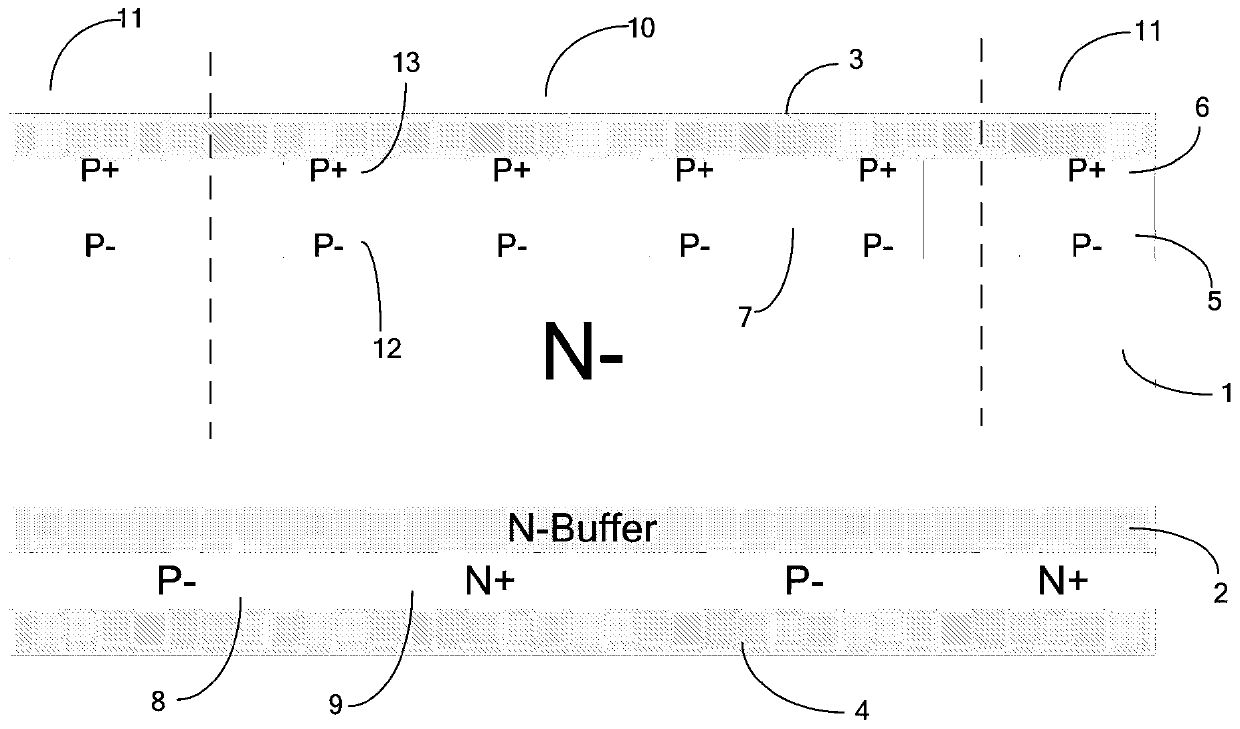
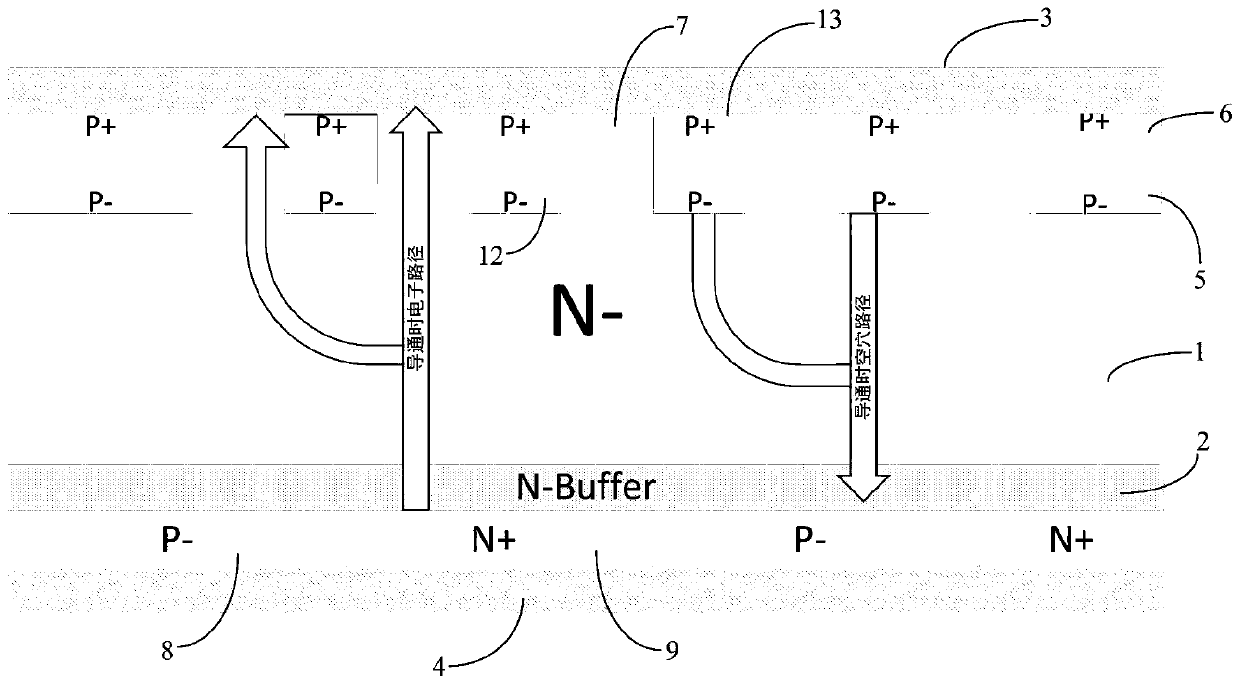
[0040] Such as figure 1 Shown: In order to obtain a faster reverse recovery time, reduce dynamic loss, improve softness, and reduce high-temperature leakage, the present invention includes a semiconductor substrate, and the semiconductor substrate includes an N-type substrate 1 and an N-type substrate. The N-type buffer layer 2 adjacent to the bottom 1 is provided with an active region 10 in the central region of the N-type substrate 1;

[0041] On the cross-section of the diode device, the active region 10 includes a number of alternately distributed active P columns and active N columns 7, the active P columns and active N columns 7 are located in the upper part of the N-type substrate 1 Anode metal 3 is set on N-type substrate 1, the active P column is in ohmic contact with anode metal 3 on N-type substrate 1, and active N column 7 is in contact with anode ...


PUM


Abstract

The invention relates to a double-sided Schottky controlled fast recovery diode device and a preparation method. The fast recovery diode device comprises a semiconductor substrate, the semiconductor substrate comprises an N-type substrate and an N-type buffer layer, and an active region is arranged in the central area of the N-type substrate. On the cross section of the diode device, the active region comprises a number of alternately distributed active P-columns and active N-columns. Anode metal is arranged on the N-type substrate. The active P-columns are in ohmic contact with the anode metal on the N-type substrate, and the active N-columns are in Schottky contact with the anode metal on the N-type substrate. A number of alternately distributed cathode P- regions and cathode N+ regionsare arranged on the N-type buffer layer, the cathode N+ regions are in ohmic contact with cathode metal, and the cathode P- regions are in Schottky contact with the cathode metal. Fast reverse recovery can be realized, the dynamic loss can be reduced, the excellent softness can be improved, and the device has high reliability.

Description

technical field [0001] The invention relates to a diode device and a preparation method, in particular to a double-sided Schottky-controlled fast recovery diode device and a preparation method, belonging to the technical field of microelectronics. Background technique [0002] With the development of power electronics technology, the application of new power electronic devices in various frequency conversion circuits and chopper circuits puts forward higher requirements for fast diodes that are connected in parallel and act as clamps or buffers to reduce diode inverse The reverse recovery charge produces the main power consumption in the power switch device, reduces the high induced voltage added to the power switch device caused by reverse recovery, and improves the service life and reliability of the power switch device. In order to achieve the above purpose, the diode must have a short reverse recovery time trr, a small reverse recovery current IRM and soft recovery chara...

Claims


Application Information

Patent Timeline
05 Nov 2019
Publication
CN110416319A
IPC
H01L29/872; H01L21/329
CPC
H01L29/872; H01L29/66143; Y02P70/50
Inventors
李磊; 许生根