A heteroepitaxial ga 2 o 3 Preparation method of thin film deep ultraviolet photodetector

A technology of heterogeneous epitaxy and electrical detectors, applied in circuits, electrical components, semiconductor devices, etc., can solve problems such as high reaction temperature, complicated process, and low utilization rate of raw materials, and achieve the effects of reducing production costs and simplifying equipment

Active Publication Date: 2021-10-29
XIDIAN UNIV
View PDF2 Cites 0 Cited by
  • Summary
  • Abstract
  • Description
  • Claims
  • Application Information

AI Technical Summary

Problems solved by technology

[0007] The object of the invention is to propose a method for making Ga 2 o 3 The method of deep ultraviolet photodetector is used to solve the uneven growth of thin films in the prior art, the low utilization rate of raw materials, the high reaction temperature and the complicated and difficult control process, so as to realize the uniform growth of large-area thin films

Method used


Image

  • A heteroepitaxial ga  <sub>2</sub> o  <sub>3</sub> Preparation method of thin film deep ultraviolet photodetector
  • A heteroepitaxial ga  <sub>2</sub> o  <sub>3</sub> Preparation method of thin film deep ultraviolet photodetector
  • A heteroepitaxial ga  <sub>2</sub> o  <sub>3</sub> Preparation method of thin film deep ultraviolet photodetector

Examples


Embodiment 1

[0028] Example 1, under the growth condition of 300°C, Ga 2 o 3 Deep ultraviolet photodetector.

[0029] Step 1, preparing an aqueous precursor solution.

[0030] Take 0.592g of gallium acetylacetonate solid powder, 80mL of deionized water, and add 0.8ml of hydrochloric acid to dissolve it in deionized water, and dissolve the gallium acetylacetonate solid powder in deionized water hydrochloric acid solution to make a concentration of 0.02mol / L. Gallium acetonate precursor aqueous solution.

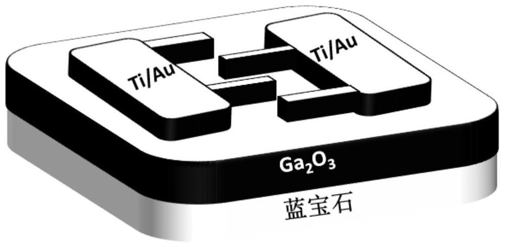
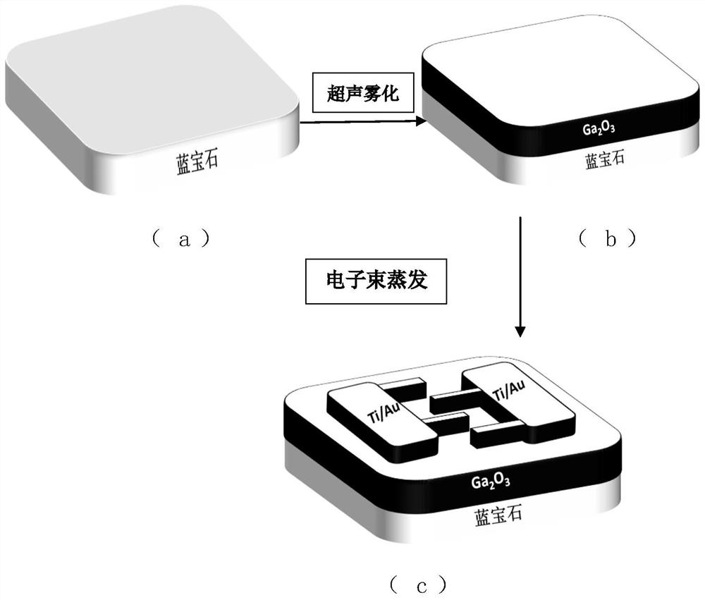
[0031] Step 2, cleaning the sapphire substrate, such as figure 2 (a).

[0032] Select the sapphire containing C face (0001) as the substrate, and clean it as follows:

[0033] Ultrasonic immersion in acetone solution for 10 minutes, then ultrasonic immersion in ethanol solution for 10 minutes, and finally ultrasonic immersion in deionized water for 10 minutes to complete the cleaning of the sapphire substrate.

[0034] Step 3, grow Ga 2 o 3 film, such as figure 2 (b).

[0035] ...

Embodiment 2

[0040] Example 2, making Ga with a thickness of 500nm under the growth condition of 550°C 2 o 3 Deep ultraviolet photodetector.

[0041] Step 1, take 1.48g of gallium acetylacetonate solid powder, 80mL of deionized water, and add 0.8ml of hydrochloric acid to dissolve in deionized water, and dissolve the gallium acetylacetonate solid powder in deionized water hydrochloric acid solution to make a concentration of 0.05mol / Aqueous solution of gallium acetylacetonate precursor in L.

[0042] Step 2, the specific implementation of this step is the same as step 2 of embodiment 1, such as figure 2 (a).

[0043] Step 3: Add the gallium acetylacetonate precursor aqueous solution to an ultrasonic nebulizer with a frequency of 1.7 MHz and atomize it into a gas, and transport the atomized gas to the reaction furnace through nitrogen. The carrier gas rate is 4 L / min, and the reaction furnace is set to The reaction temperature is 550°C, and the reaction time is 50 minutes. The atomize...

Embodiment 3

[0046] Example 3, making a Ga with a thickness of 2000nm under the growth condition of 800°C 2 o 3 Deep ultraviolet photodetector.

[0047] Step A, take 5.92 g of gallium acetylacetonate solid powder, 80 mL of deionized water, and add 0.8 ml of hydrochloric acid to dissolve in deionized water, and dissolve the gallium acetylacetonate solid powder in deionized water hydrochloric acid solution to make a concentration of 0.2 mol / Aqueous solution of gallium acetylacetonate precursor in L.

[0048] Step B, cleaning sapphire substrate: the specific implementation of this step is the same as step 2 of embodiment 1, as figure 2 (a).

[0049] Step C, adding the gallium acetylacetonate precursor aqueous solution to an ultrasonic nebulizer with a frequency of 1.7 MHz to atomize it into a gas, and transport the atomized gas to the reaction furnace through oxygen, the carrier gas rate is 8 L / min, and the reaction furnace is set to The reaction temperature is 800°C, and the reaction t...


PUM

PropertyMeasurementUnit
thicknessaaaaaaaaaa
thicknessaaaaaaaaaa
thicknessaaaaaaaaaa

Abstract

The invention discloses a Ga 2 o 3 The preparation method of the deep ultraviolet detector mainly solves the problems of high reaction temperature and complex equipment process in the prior art. The implementation plan is: 1. Prepare the precursor gallium acetylacetonate aqueous solution; 2. Clean the sapphire substrate; 3. Ultrasonic atomize the precursor gallium acetylacetonate aqueous solution through Mist-Cvd equipment, and put it on the cleaned sapphire substrate Heating grows to Ga 2 o 3 thin film; 4. Ga 2 o 3 Make electrode pattern on the sample of thin film; 5. On the Ga with electrode pattern 2 o 3 Fabricate metal electrodes on the film to complete the Ga 2 o 3 Fabrication of deep ultraviolet detectors. The process of the invention is simple and easy to realize, that is, a high-quality thin film can be obtained in a short time only at a relatively low synthesis temperature. Photoelectric tests show that the deep ultraviolet photodetector made by the invention has high responsivity and fast response time, and can be used in the preparation of detectors.

Description

technical field [0001] The invention belongs to the technical field of semiconductor devices, in particular to a method for preparing a photodetector, which can be used for Ga 2 o 3 Fabrication of thin-film deep-ultraviolet detectors. Background technique [0002] With the continuous development of modern semiconductor photoelectric detection technology, ultraviolet rays, especially 200-280nm solar-blind ultraviolet rays, are absorbed by the ozone layer when they enter the atmosphere. Solar-blind ultraviolet detection can eliminate the concerns of interference and achieve efficient and accurate detection. Solar-blind photoelectric detection There are a growing number of military and civilian surveillance applications, such as missile tracking, secure communications, fire detection, ozone hole monitoring, chemical, biological analysis, and corona detection. Ga 2 o 3 It is a wide bandgap compound semiconductor material. Its forbidden band width is between 4.5 and 4.9eV, s...

Claims


Application Information

Patent Timeline
Patent Type & Authority Patents(China)
IPC IPC(8): H01L31/032H01L31/108H01L31/18
CPCH01L31/032H01L31/108H01L31/18Y02P70/50
Inventor 张春福许育安志远张进成郝跃陈大正
Owner XIDIAN UNIV
Why Eureka
Try Eureka