GaN-based heterojunction field effect transistor and manufacturing method thereof

A technology of heterojunction field effect and manufacturing method, which is applied in semiconductor/solid-state device manufacturing, semiconductor devices, electrical components, etc., and can solve problems that cannot meet the requirements of high-frequency and high-voltage applications.

Pending Publication Date: 2019-11-12
THE 13TH RES INST OF CHINA ELECTRONICS TECH GRP CORP
View PDF14 Cites 4 Cited by
  • Summary
  • Abstract
  • Description
  • Claims
  • Application Information

AI Technical Summary

Problems solved by technology

[0004] In view of this, an embodiment of the present invention provides a GaN-based heterojunction field-effect transistor and a manufacturing method thereof to solve the problem that the GaN-based heterojunction field-effect transistor in the prior art cannot meet the high-frequency and high-voltage applications.

Method used


Image

  • GaN-based heterojunction field effect transistor and manufacturing method thereof
  • GaN-based heterojunction field effect transistor and manufacturing method thereof
  • GaN-based heterojunction field effect transistor and manufacturing method thereof

Examples


Embodiment Construction

[0024] In order to make the technical problems, technical solutions and beneficial effects to be solved by the present invention clearer, the present invention will be further described in detail below in conjunction with the accompanying drawings and embodiments. It should be understood that the specific embodiments described here are only used to explain the present invention, not to limit the present invention.

[0025] The present invention will be further described in detail below in conjunction with the accompanying drawings and specific embodiments.

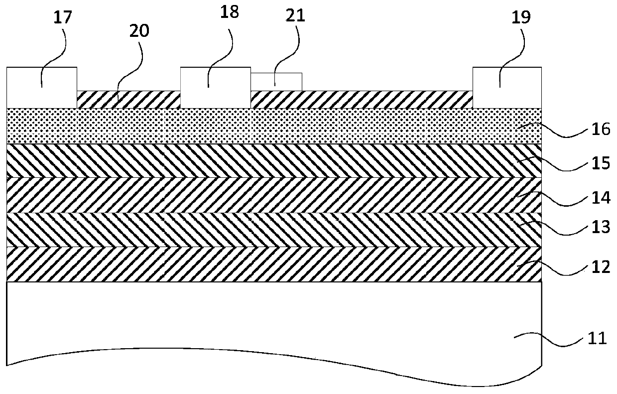
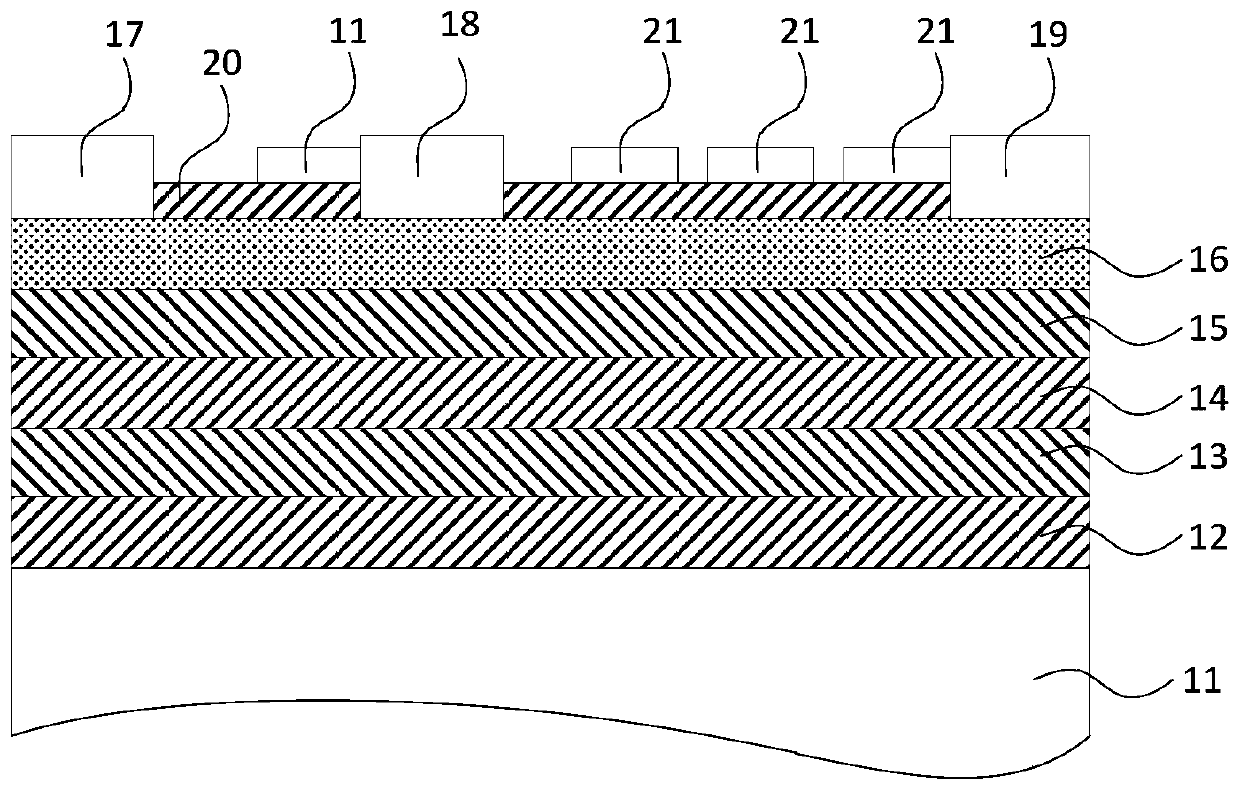
[0026] refer to figure 1 , an embodiment of the present invention provides a GaN-based heterojunction field effect transistor, which sequentially includes a substrate 11, a nucleation layer 12, a buffer layer 13, a channel layer 14, an insertion layer 15, and a barrier layer from bottom to top 16 and a source 17 , a gate 18 and a drain 19 arranged on the barrier layer 16 . A passivation layer 20 is disposed on the barrie...


PUM


Abstract

The invention is applicable to the technical field of semiconductor devices, and particularly relates to a GaN-based heterojunction field effect transistor and a manufacturing method thereof. The transistor sequentially comprises a substrate, a nucleating layer, a buffer layer, a channel layer, an insertion layer, a barrier layer, a source electrode, a grid electrode and a drain electrode from bottom to top, wherein the source electrode, the grid electrode and the drain electrode are arranged on the barrier layer. Passivation layers are arranged between the source electrode and the grid electrode and between the grid electrode and the drain electrode on the barrier layer. Field plates are arranged on the passivation layers. The forming material of the barrier layer includes: B (Al, Ga, In)N. The forbidden band width of the barrier layer is larger than the forbidden band width of the channel layer and smaller than the forbidden band width of the insertion layer. A heterojunction interface formed by the barrier layer made of the B (Al, Ga, In) N materials is large in band gap difference. The barrier layer has super-large polarization field intensity, very high two-dimensional electron gas concentration can be obtained, and the high-frequency requirement of a device is met. Through the field plates, the electric field peak value of the grid edge can be reduced, the channel electric field distribution uniformity of the device is improved, the breakdown voltage of the device is increased and the high-voltage requirements are met.

Description

technical field [0001] The invention belongs to the technical field of semiconductor devices, and in particular relates to a GaN-based heterojunction field effect transistor and a manufacturing method thereof. Background technique [0002] GaN-based heterojunction field-effect transistors have a wide band gap, high critical breakdown electric field, high output power, and high efficiency, and have broad application prospects. [0003] With the demand for device miniaturization, when the GaN barrier layer is reduced to below 12nm, it is difficult to achieve a high two-dimensional electron gas (2DEG) density in the channel, which cannot meet the needs of the device. The increasingly serious short channel effect limits GaN The application of HFETs devices in high-frequency devices and ultra-high-speed circuits above the W-band. At the same time, when the device withstands the withstand voltage, the channel depletion region will expand to the drain, and the electric force lines...

Claims


Application Information

Patent Timeline
Patent Type & Authority Applications(China)
IPC IPC(8): H01L29/778H01L29/20H01L29/205H01L21/335
CPCH01L29/7786H01L29/7787H01L29/2003H01L29/205H01L29/66462
Inventor 郭艳敏房玉龙尹甲运李佳王波张志荣芦伟立高楠王元刚冯志红
Owner THE 13TH RES INST OF CHINA ELECTRONICS TECH GRP CORP
Why Eureka
Try Eureka