Silicon substrate cleaning method

A silicon substrate, physical cleaning technology, used in electrical components, carbon nanotubes, semiconductor/solid-state device manufacturing, etc., can solve the problems of poor cleaning effect of carbon nanotube root residues, easy to corrode oxide layers, etc., and achieve large-scale promotion. Value, uniform array height, good cleaning effect

Active Publication Date: 2019-11-15
CONE SCI CITY GUANGZHOU ADVANCED MATERIALS CO LTD
View PDF4 Cites 0 Cited by
  • Summary
  • Abstract
  • Description
  • Claims
  • Application Information

AI Technical Summary

Problems solved by technology

[0005] The object of the present invention is to provide a cleaning method for a silicon substrate, aiming at solving the problem that the existing cleaning technology is easy to corrode and damage the oxide layer on the surface of the silicon substrate, and the cleaning effect of the carbon nanotube root residue on the surface of the silicon substrate is not good

Method used


Image

  • Silicon substrate cleaning method
  • Silicon substrate cleaning method
  • Silicon substrate cleaning method

Examples


Embodiment 1

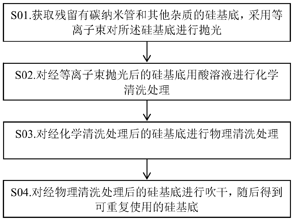
[0063] 200 8-inch silicon substrates with residual carbon nanotubes and other impurities were obtained, and the silicon substrates were polished with a plasma beam. Specifically, the silicon substrate is horizontally placed on the conveyor belt of the plasma cleaning machine, so that the side on which the carbon nanotubes grow is in contact with the conveyor belt, so that the conveyor belt is polished by the ion beam ejected from the plasma emission head along with the conveyor belt, The ion beam loosens the carbon nanotubes and amorphous carbon attached to the surface of the silicon substrate. The speed of the conveyor belt of the plasma cleaning machine is 33 mm / s; the speed of the plasma axis is 500 mm / s. The plasma beam polished silicon substrate is chemically cleaned with an acid solution, the acid solution is an SPM acid solution, and the cleaning treatment is performed at a temperature of 110° C. for 15 minutes. Wherein, the SPM acid solution is a mixed solution of conc...

Embodiment 2

[0065]200 8-inch silicon substrates with residual carbon nanotubes and other impurities were obtained, and the silicon substrates were polished with a plasma beam. Specifically, the silicon substrate is horizontally placed on the conveyor belt of the plasma cleaning machine, so that the side on which the carbon nanotubes grow is in contact with the conveyor belt, so that the conveyor belt is polished by the ion beam ejected from the plasma emission head along with the conveyor belt, The ion beam loosens the carbon nanotubes and amorphous carbon attached to the surface of the silicon substrate. The speed of the conveyor belt of the plasma cleaning machine is 32 mm / s; the speed of the plasma axis is 498 mm / s. The plasma beam polished silicon substrate is chemically cleaned with an acid solution, the acid solution is an HPM acid solution, and the cleaning treatment is carried out at a temperature of 70° C. for 15 minutes. Wherein, the HPM acid solution is a mixed solution of deio...

Embodiment 3

[0067] 200 8-inch silicon substrates with residual carbon nanotubes and other impurities were obtained, and the silicon substrates were polished with a plasma beam. Specifically, the silicon substrate is horizontally placed on the conveyor belt of the plasma cleaning machine, so that the side on which the carbon nanotubes grow is in contact with the conveyor belt, so that the conveyor belt is polished by the ion beam ejected from the plasma emission head along with the conveyor belt, The ion beam loosens the carbon nanotubes and amorphous carbon attached to the surface of the silicon substrate. The speed of the conveyor belt of the plasma cleaning machine is 34 mm / s; the speed of the plasma axis is 504 mm / s. The plasma beam polished silicon substrate is chemically cleaned with an acid solution, the acid solution is a hydrochloric acid solution, and the cleaning treatment is carried out at a temperature of 70° C. for 15 minutes. Wherein, the hydrochloric acid solution is a hydr...


PUM


Abstract

The invention provides a silicon substrate cleaning method. The silicon substrate cleaning method comprises steps that the silicon substrate with carbon nanotubes and other impurities remaining is obtained, and the silicon substrate is polished through plasma beams; the silicon substrate after plasma beam polishing is chemically cleaned with acid solution; and silicon substrate after chemical cleaning is subjected to physical cleaning; the silicon substrate physical cleaning is blown dry, and then a reusable silicon substrate is obtained. The method is advantaged in that the silicon surface color is uniform and consistent after cleaning, a spot and ash stamp problem is eliminated, and the secondary carbon nanotube growth test shows that the carbon nanotube output reaches 92-98% of new silicon wafers, which basically met target requirements.

Description

technical field [0001] The invention belongs to a silicon chip cleaning process, in particular to a cleaning method for a silicon substrate with carbon nanotube residues on the surface. Background technique [0002] In recent years, with the in-depth research on carbon nanotubes and nanomaterials, the demand for carbon nanotubes is increasing, and its broad application prospects are constantly showing. Carbon nanotubes, also known as bucky tubes, are one-dimensional quantum materials with a special structure (the radial dimension is on the order of nanometers, the axial dimension is on the order of microns, and both ends of the tube are basically sealed). Carbon nanotubes are mainly coaxial tubes with several to tens of layers of carbon atoms arranged in a hexagonal shape. A fixed distance is maintained between layers, about 0.34nm, and the diameter is generally 2 to 20nm. And according to the different orientations of the carbon hexagon along the axial direction, it can b...

Claims


Application Information

Patent Timeline
IPC IPC(8): H01L21/02C01B32/16
CPCC01B32/16H01L21/02054H01L21/02079
Inventor 辛培培
Owner CONE SCI CITY GUANGZHOU ADVANCED MATERIALS CO LTD
Why Eureka
Try Eureka