A kind of ultraviolet LED chip and preparation method thereof
An LED chip and ultraviolet technology, applied in semiconductor devices, electrical components, circuits, etc., can solve the problems of weak resistance to high humidity aging, discounted brightening effect, poor heat dissipation effect, etc., to slow down aging failure, high waterproof, The effect of increasing the brightness
- Summary
- Abstract
- Description
- Claims
- Application Information
AI Technical Summary
Problems solved by technology
Method used
Image
Examples
Embodiment 1
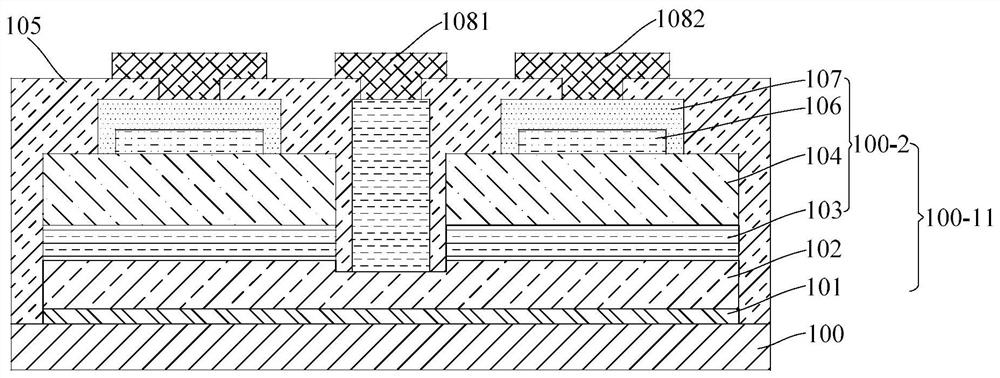
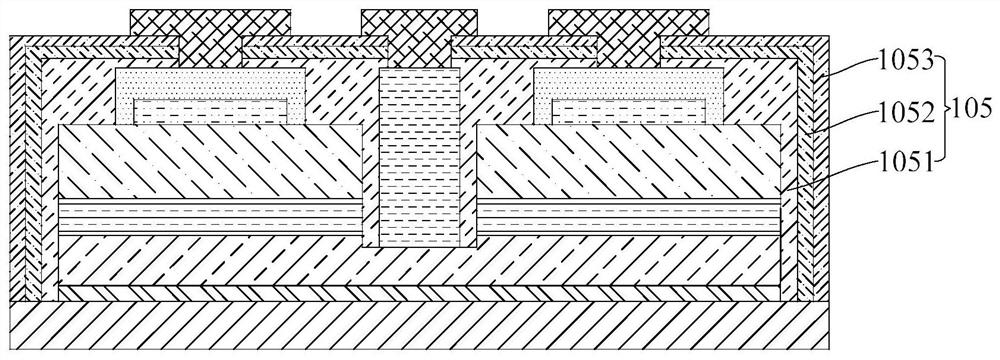
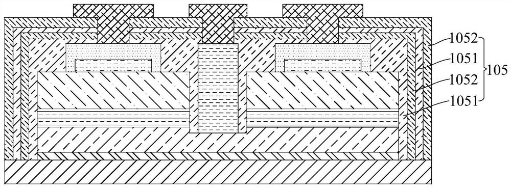
[0065] Such as Figure 1-4 As shown, in this embodiment, the light-emitting epitaxial layer 100-11 is formed above the substrate 100, and the light-emitting epitaxial layer includes a first semiconductor layer 102, an active layer 103, and a first semiconductor layer sequentially formed above the substrate 100. The second semiconductor layer 104 of opposite conductivity type. The above-mentioned first semiconductor layer 102 forms the first mesa 100-1 of the light-emitting epitaxial layer 100-11 (refer to the attached Figure 4 As shown), the active layer 103 and the second semiconductor layer 104 form the second mesa 100-2 of the light emitting epitaxial layer 100-11.
[0066] In a preferred embodiment of this embodiment, the substrate may be a sapphire substrate, the first semiconductor layer 102 may be an N-type semiconductor layer, and the N-type semiconductor layer may include, for example, an AlN / AlGaN superlattice layer, The heavily doped N-type AlGaN layer, the light...
Embodiment 2
[0076] This embodiment also provides a method for preparing an ultraviolet LED chip, such as Figure 4 As shown, the method includes the following steps:
[0077] forming a light-emitting epitaxial layer, sequentially depositing a first semiconductor layer, an active layer, and a second semiconductor layer having a conductivity type opposite to that of the first semiconductor layer, the first semiconductor layer forming a first mesa of the light-emitting epitaxial layer, The active layer and the second semiconductor layer form a second mesa of the light emitting epitaxial layer;
[0078] An insulating protection layer is formed above the light-emitting epitaxial layer, the insulating protection layer covers the surface and side surfaces of the first mesa and the second mesa, and the insulating protection layer includes an insulating layer containing Al.
[0079] The light-emitting epitaxial layer can be formed by methods commonly used in the art. Such as Figure 5 As shown,...
PUM
| Property | Measurement | Unit |
|---|---|---|
| refractive index | aaaaa | aaaaa |
| refractive index | aaaaa | aaaaa |
| refractive index | aaaaa | aaaaa |
Abstract
Description
Claims
Application Information


