Method and device for reducing positional deviation between chip embedding and photolithographic pattern
A chip and graphics technology, used in semiconductor/solid-state device testing/measurement, semiconductor devices, electrical components, etc., can solve the problems of inaccurate alignment of chip pin patterns, short circuits, embedded chip errors, etc., to improve packaging technology, Simple process steps
- Summary
- Abstract
- Description
- Claims
- Application Information
AI Technical Summary
Problems solved by technology
Method used
Image

Examples
Embodiment
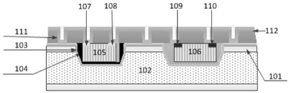
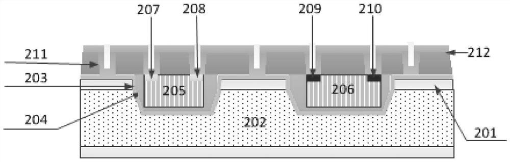
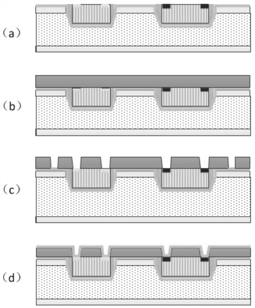
[0036] (a) take a 500 μm thick 3-inch high-resistance round silicon wafer as the substrate 202, and etch SiO 2 The film 201 is opened, the chip groove and the electroplated metal formation 203 are made, a small amount of conductive silver paste 204 is applied for fixing and conducting, and the chips (205, 206) are embedded, and the surfaces of all chips and silicon chips are basically flat, such as image 3 as shown in (a);
[0037] (b) Use a visible light three-dimensional microscope to take pictures of all embedded chips at a magnification of 20 times, import the pictures into AutoCAD drawing software, and draw the chips and their pins after scaling down, and use the chip of each chip Based on the groove, draw each embedded chip and its pins on the mask plate of the entire wafer, and then draw the mask plate of the dielectric via hole on the upper layer of the chip and the mask plate of the metal layer wiring and passive devices;
[0038] (c) Apply photoresist, such as im...
PUM
 Abstract
Description
Claims
Application Information