Contact plug, semiconductor device and method of manufacturing the same

A contact plug and manufacturing method technology, which is applied in the fields of semiconductor/solid-state device manufacturing, semiconductor devices, semiconductor/solid-state device parts, etc. The effect of reducing contact resistance

Active Publication Date: 2021-10-01
SEMICON MFG INT (SHANGHAI) CORP +1
View PDF0 Cites 0 Cited by
  • Summary
  • Abstract
  • Description
  • Claims
  • Application Information

AI Technical Summary

Problems solved by technology

However, with the increasing integration of integrated circuits, the contact plugs formed by the current contact plug manufacturing methods cannot meet the manufacturing requirements of higher-performance FinFET devices.

Method used


Image

  • Contact plug, semiconductor device and method of manufacturing the same
  • Contact plug, semiconductor device and method of manufacturing the same
  • Contact plug, semiconductor device and method of manufacturing the same

Examples


Embodiment Construction

[0045] A method of manufacturing a contact plug, comprising the steps of:

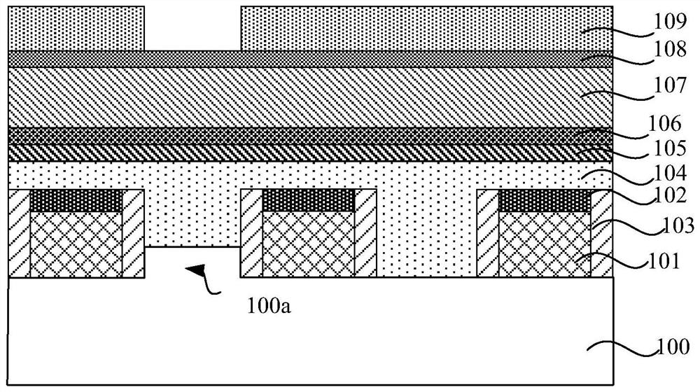
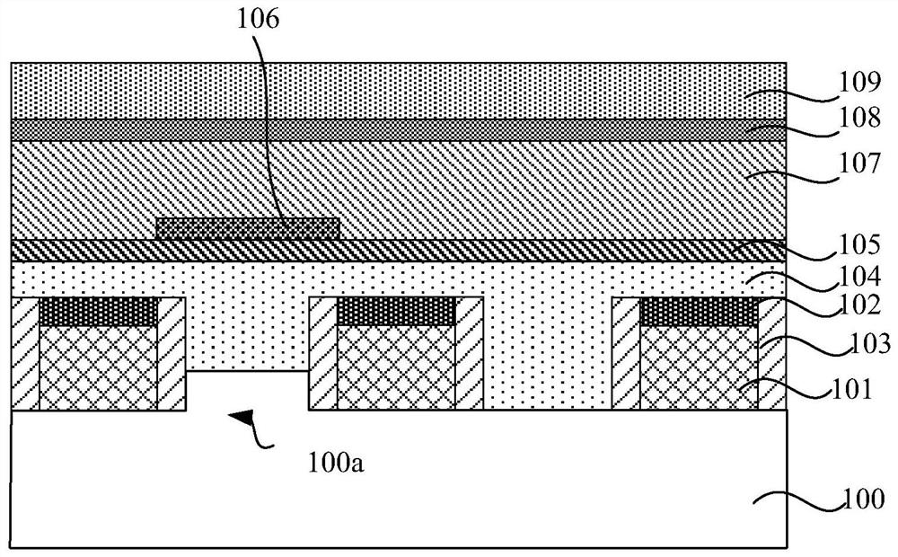
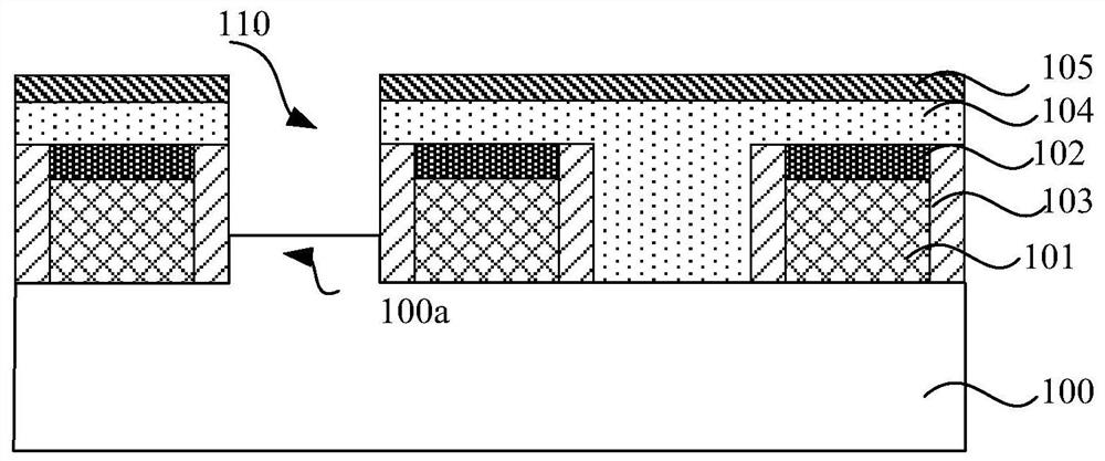
[0046] First, please refer to Figure 1A , 1B and Figure 2A , provide a semiconductor substrate 100, a gate structure 101 (which may be a polysilicon gate structure or a high-K metal gate structure) is formed on the semiconductor substrate 100, and the top of the gate structure 101 is covered with A silicon nitride mask layer 102, sidewalls 103 are formed on the sidewalls of the gate structure 102 and the silicon nitride mask layer 102, and fins 100a are formed in the semiconductor substrate 100 (which may be formed by embedded source-drain epitaxy source or drain region formed by the process);

[0047] Then, please continue to refer to Figure 1A , 1B and Figure 2A , depositing a sufficiently thick interlayer dielectric layer 104 on the surfaces of the semiconductor substrate 100, sidewalls 103, and silicon nitride mask layer 102, and planarizing the top of the interlayer dielectric layer 104;...


PUM


Abstract

The invention provides a contact plug, a semiconductor device and a manufacturing method thereof, which can realize the manufacture of a replacement contact plug, and can cover only the area to be contacted of the structure to be contacted with the assistance of a filling layer. The dummy contact is removed to form a contact trench at the position of the dummy contact, and a dielectric spacer is formed on the sidewall of the contact trench, and then a conductive material layer is filled in the space of the contact trench surrounded by the dielectric sidewall , to form contact plugs, this alternative process can reduce the difficulty of forming contact plugs, improve the quality of the formed contact plugs, and can increase the contact area of ​​the formed contact plugs by reducing the thickness of the dielectric sidewall , reducing contact resistance, suitable for the manufacture of contact plugs on gates, source and drain regions, body regions and other contact structures, and can improve the performance of corresponding contact plugs and semiconductor devices.

Description

technical field [0001] The invention relates to the technical field of integrated circuit manufacturing, in particular to a contact plug, a semiconductor device and a manufacturing method thereof. Background technique [0002] MOSFET (Metal Oxide Semiconductor Field Effect Transistor) is the main building block of most semiconductor devices. As the size of semiconductor devices becomes smaller and smaller (scaling continues below the 14nm node), the distance between the drain and the source is also shortened. The short-channel effect becomes more and more obvious, the control ability of the gate to the channel becomes worse, and it becomes more and more difficult for the gate voltage to pinch off the channel, and it is more likely to cause subthrehhold leakage (Subthrehhold leakage). In order to suppress the short channel effect, it is proposed to form a Fin Field Effect Transistor (Fin Field effect transistor, FinFET) on an SOI wafer or a bulk semiconductor substrate. The ...

Claims


Application Information

Patent Timeline
Patent Type & Authority Patents(China)
IPC IPC(8): H01L21/768H01L23/535H01L29/78
CPCH01L21/76895H01L23/535H01L29/785H01L2029/7858
Inventor 张海洋刘少雄钟伯琛
Owner SEMICON MFG INT (SHANGHAI) CORP
Why Eureka
Try Eureka