Artificial surface plasmon transmission line based on fractal branch structure and its application thereof
An artificial surface plasma and transmission line technology, applied in electrical components, waveguides, circuits, etc., can solve the problems of limited integrated circuit application and large size, and achieve the effect of strong electromagnetic wave restraint performance, small structure size, and excellent transmission characteristics.
- Summary
- Abstract
- Description
- Claims
- Application Information
AI Technical Summary
Problems solved by technology
Method used
Image

Examples
Embodiment 1
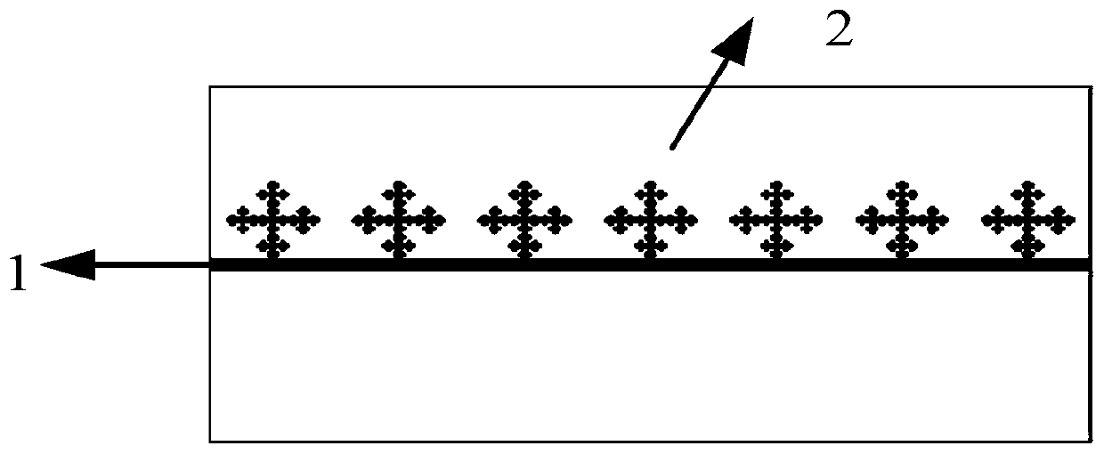
[0028] Such as figure 1 As shown, the artificial surface plasmon transmission line includes a microstrip line 1, and a periodic fractal branch 2 is arranged on the central strip of the microstrip line, and the periodic fractal branch 2 is distributed on one side of the central strip of the microstrip line.
[0029] In this embodiment, the dielectric substrate material of the microstrip line is Rogers RT5880, the dielectric constant is 2.2, the thickness is 0.508mm, and the transmission loss angle is 0.0009; the material of the metal film transmission line and the periodic fractal branches is copper.
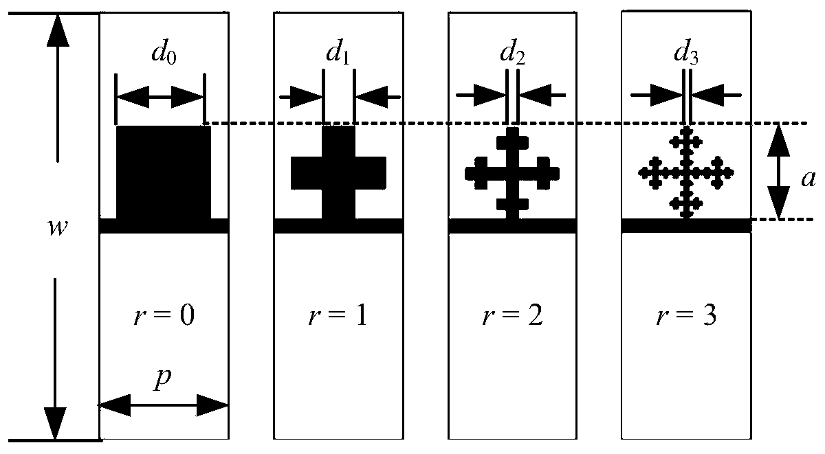
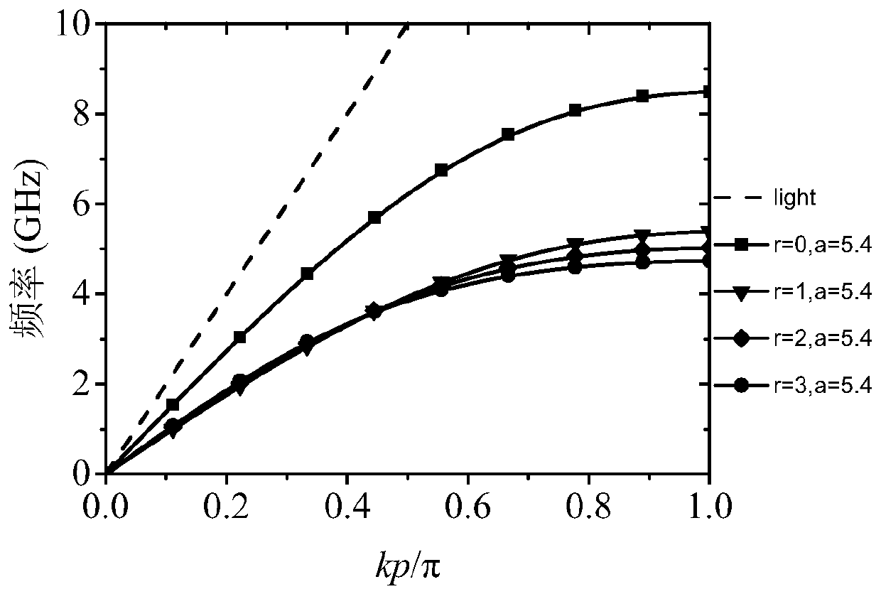
[0030] Each periodic unit structure of the artificial surface plasmon transmission line is as follows figure 2 As shown, they are the shapes of the fractal branches of the periodic unit structure after different iterations, and the dimensions are selected as: w=25mm, p=7.5mm, a=5.4mm, d r =a-r(r=0,1,2,3), where w represents the substrate width, p represents the period, a repres...
Embodiment 2
[0033] Such as Figure 4 As shown, embodiment 2 is an artificial surface plasmon transmission line designed based on embodiment 1, including a microstrip line 1, and a periodic fractal branch 2 is arranged on the central strip of the microstrip line, and the periodic fractal branch 2 is distributed On both sides of the central strip of the microstrip line;
[0034] Specifically, both ends of the artificial surface plasmon transmission line are microstrip feeding ends, and the microstrip line width is w 1 =1.54mm, to ensure a port impedance of 50Ω, design a transition structure of 6 periods through a and r to achieve impedance matching, and the parameters are designed as follows: the first transition period 3, r = 2, a = 4.9mm; the second transition period Period 4, r=2, a=3.9mm; third transition period 5, r=1, a=3.2mm; fourth transition period 6, r=1, a=2.4mm; fifth transition period 7 , r=0, a=1.4mm; the sixth transition period 8, r=0, a=1.2mm; other main parameters are as ...
Embodiment 3
[0037] Such as Figure 6 As shown, Embodiment 3 is a power splitter designed based on Embodiment 2. The power splitter is mainly composed of a straight waveguide 9 and two curved waveguides 10, wherein the straight waveguide 9 is divided into two at the bifurcation part 11, Rotate α=30° through 4 cycles respectively to form two curved waveguides 10, and load a 100Ω resistor 12 at β=15° in the middle 2 cycles, and the power divider also includes three ports, which are respectively port one 14, Port 2 15 and port 3 16, in which port 2 15 and port 3 16 are respectively connected to the transition section 13 between the microstrip and the curved waveguide, and the parameters are set as: port microstrip line width w 1 =1.54mm, microstrip line width w in curved waveguide 0 =0.77mm, to achieve impedance matching, other main parameters are as follows: substrate width w 2 =60mm, length of transition section l 5 =10mm, total length of power divider l 4 = 214.8mm. Depend on Figure...
PUM
 Abstract
Description
Claims
Application Information
 - Generate Ideas
- Intellectual Property
- Life Sciences
- Materials
- Tech Scout
- Unparalleled Data Quality
- Higher Quality Content
- 60% Fewer Hallucinations
Browse by: Latest US Patents, China's latest patents, Technical Efficacy Thesaurus, Application Domain, Technology Topic, Popular Technical Reports.
© 2025 PatSnap. All rights reserved.Legal|Privacy policy|Modern Slavery Act Transparency Statement|Sitemap|About US| Contact US: help@patsnap.com