

Electron microscopic imaging system and imaging method
An electron microscope and imaging system technology, applied in the direction of circuits, discharge tubes, electrical components, etc., can solve the problems of reducing imaging quality and sample damage, and achieve the effect of improving acquisition efficiency, improving efficiency, and improving quality
- Summary
- Abstract
- Description
- Claims
- Application Information
AI Technical Summary
Problems solved by technology
Method used
Image

Examples
Embodiment 1
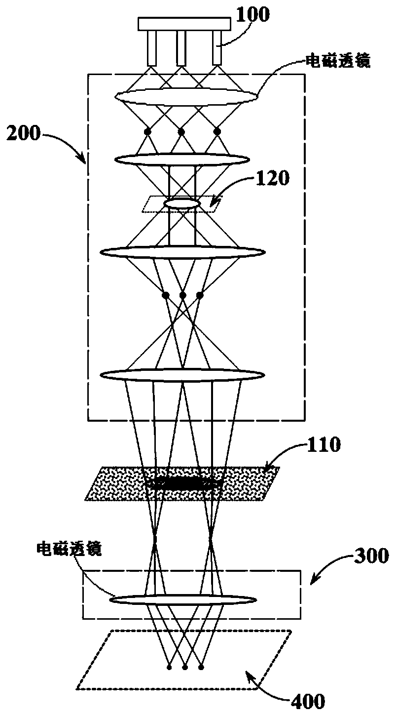
[0035] to combine figure 1 As shown, an electron microscopic imaging system of the present invention includes several charged particle sources 100, and the charged particle sources 100 are used to emit charged particles. It is worth noting that several charged particle sources 100 are at the same height, and several charged particle sources 100 can be controlled independently, so that any number of charged particle sources 100 can be controlled to emit charged particles; especially, this The several charged particle sources 100 of the invention can be arranged arbitrarily, for example, the charged particle sources 100 can be arranged in an array, specifically, several charged particle sources 100 can be arranged in a regular shape such as a circle or a rectangle. By arranging several charged particle sources 100, arrayed charged particle beams can be obtained under single irradiation.
[0036] In addition, an electron microscopic imaging system of the present invention also i...
Embodiment 2
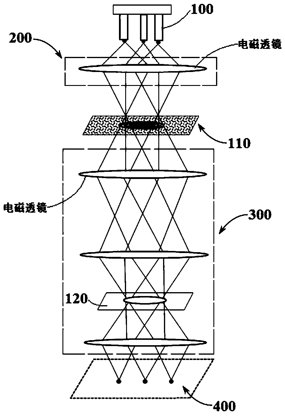
[0040] to combine figure 2 As shown, the content of this embodiment is basically the same as that of Embodiment 1, the difference being that: the converging unit 200 of this embodiment is not provided with an aperture 120, and the converging unit 200 is only provided with an electromagnetic lens; the diffraction of this embodiment The unit 300 includes three electromagnetic lenses, the three electromagnetic lenses are respectively electromagnetic lens a, electromagnetic lens b, and electromagnetic lens c from top to bottom, and an aperture 120 is arranged between the electromagnetic lens b and the electromagnetic lens c, and the aperture 120 Located on the focal plane or the conjugate plane of the focal plane; the aperture 120 can limit the collection angle of the diffraction pattern, and the aperture 120 of this embodiment is located on the conjugate plane of the focal plane; and the focal plane is defined by the converging unit 200 form.
[0041] Through the above settings...
Embodiment 3
[0043] An electron microscopic imaging method of the present invention adopts the above-mentioned electron microscopic imaging system, several charged particle sources 100 emit charged particles to form several charged particle beams, and several charged particle beams pass through the converging unit 200 forms overlapping charged particle beam probes, penetrates the sample 110 and forms a set of diffraction patterns of the sample 110 through the diffraction unit 300, and the detector 400 receives the set of diffraction patterns and performs stacked imaging to reconstruct the image of the sample 110. It is worth noting that the position arrangement of the sample 110 irradiated by the charged particle beam probe corresponds to the position arrangement of the charged particle source 100; and a diffraction image carrying the image of the sample 110 in a single irradiation can be divided into A set of diffraction images of the position where the electron particle beam probe is illu...
PUM
 Abstract
Description
Claims
Application Information