
Eureka
For R&D, Eureka makes reading and utilizing patents & technical documents easy.
Eureka AIR
Designed for self-driven R&D workflows. Generate viable solutions, solve complex R&D challenges, empower your innovation with AI.

Eureka Materials
Designed for material experts only. Revolutionize your material R&D, from search, analyze, to developing new materials.

TechResearch
Generate reliable direction feasibility study reports for your R&D in just a few steps.

TechSeek
Discover and master advanced knowledge NOW. Basics, ideas, possibilities, all at once.

TechMind
As an expert in R&D Theories, TechMind can generates customized viable solutions instantly.

TechRisk
Analyze your overall solution with one click, know your potential R&D risks in advance.

TechMonitor
Get weekly tech updates, stay abreast of the latest tech innovations and key insights.
Method for manufacturing silicon single crystal ingot and silicon single crystal growing apparatus
A monocrystalline silicon ingot and a manufacturing method technology, applied in the field of monocrystalline silicon cultivation devices, capable of solving the problems of low yield of n-type monocrystalline silicon ingots and the like
- Summary
- Abstract
- Description
- Claims
- Application Information
AI Technical Summary
Problems solved by technology
Method used
Image

Examples
Embodiment
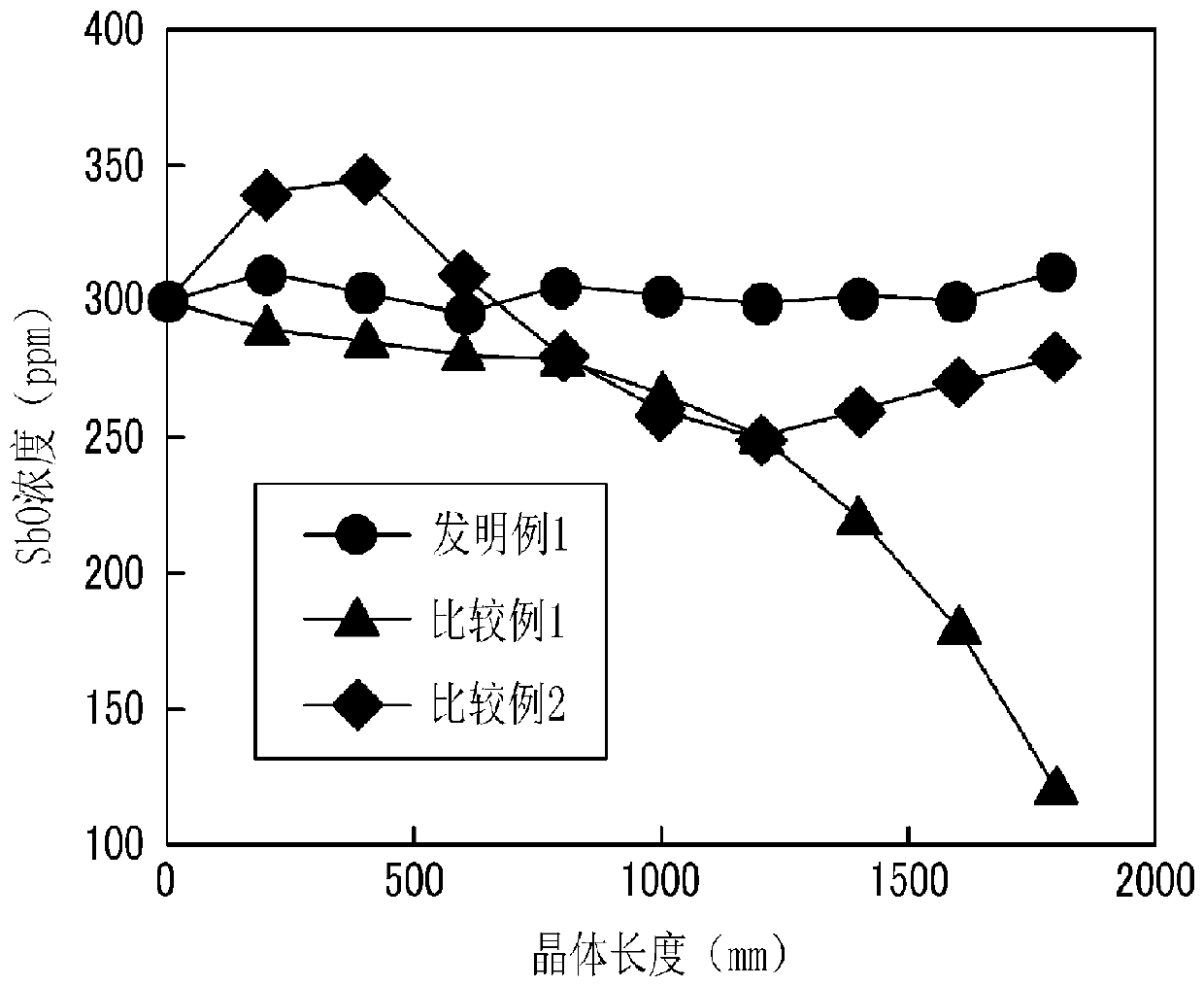
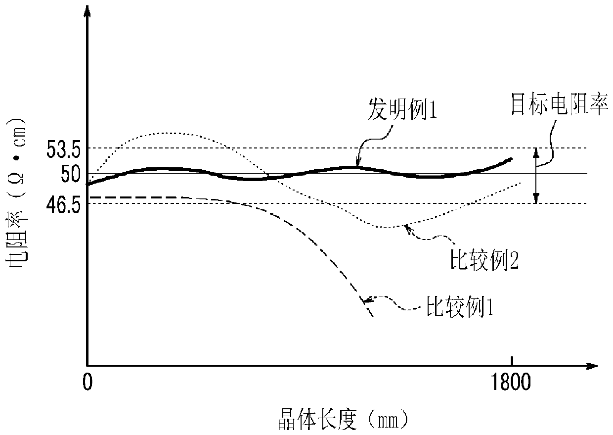
[0088] Next, in order to further clarify the effects of the present invention, the following examples are given, but the present invention is not limited by the following examples.
[0089] (Invention Example 1)
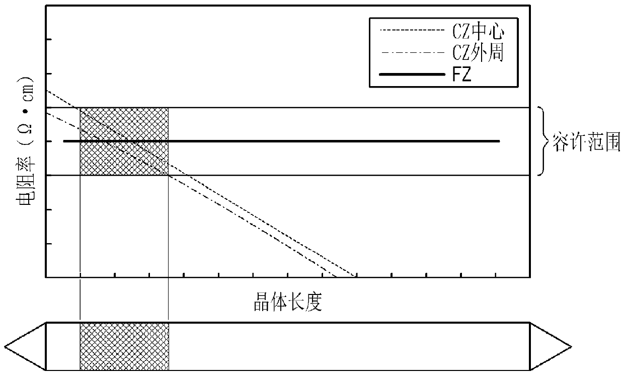
[0090] use figure 2 The single crystal silicon growing device 100 shown grows a single crystal silicon ingot with a diameter of 300 mm and a straight body length of 1800 mm by the CZ method. First, 350 kg of a polycrystalline silicon raw material was put into a 32-inch quartz crucible 20, and the polycrystalline silicon raw material was dissolved in an argon atmosphere. Next, Sb (antimony) was added as an n-type dopant. At this time, the dopant dose was adjusted so that the resistivity at the starting position of the straight body of the single crystal silicon ingot became 50 Ω·cm. In addition, the target resistivity of the crystal was set to 50Ω·cm±7% in the axial direction. Then, the seed crystal is immersed in the silicon melt 10, and the seed crystal is grad...
PUM
| Property | Measurement | Unit |
|---|---|---|
| diameter | aaaaa | aaaaa |
| diameter | aaaaa | aaaaa |
| electrical resistivity | aaaaa | aaaaa |
Abstract
Description
Claims
Application Information
 - R&D Engineer
- R&D Manager
- IP Professional
- Industry Leading Data Capabilities
- Powerful AI technology
- Patent DNA Extraction
Browse by: Latest US Patents, China's latest patents, Technical Efficacy Thesaurus, Application Domain, Technology Topic, Popular Technical Reports.
© 2024 PatSnap. All rights reserved.Legal|Privacy policy|Modern Slavery Act Transparency Statement|Sitemap|About US| Contact US: help@patsnap.com