Lateral root-enhanced junction field effect transistor device and its preparation method

A field effect transistor and enhancement mode technology, applied in the field of lateral GaN-based enhancement mode junction field effect transistors, can solve the problems of increasing the difficulty of driving circuit design, increasing the off-state loss of power semiconductor devices, etc., to achieve high current output, increase Off-state loss, the effect of simplifying the drive circuit

Active Publication Date: 2021-03-02
NANJING UNIV
View PDF6 Cites 0 Cited by
  • Summary
  • Abstract
  • Description
  • Claims
  • Application Information

AI Technical Summary

Problems solved by technology

JFET is generally a depletion-type device, and the gate can only work normally when a reverse voltage is applied to the gate. For power electronics applications, power semiconductor devices are often required to be enhanced devices, otherwise it will increase the difficulty of driving circuit design and increase Off-state loss of high-power semiconductor devices

Method used


Image

  • Lateral root-enhanced junction field effect transistor device and its preparation method
  • Lateral root-enhanced junction field effect transistor device and its preparation method
  • Lateral root-enhanced junction field effect transistor device and its preparation method

Examples


Embodiment 1

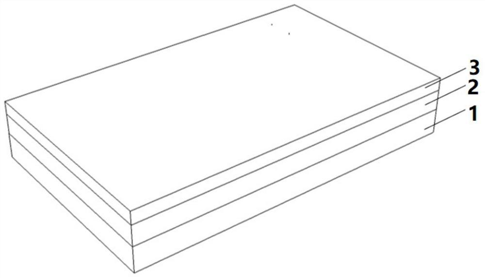
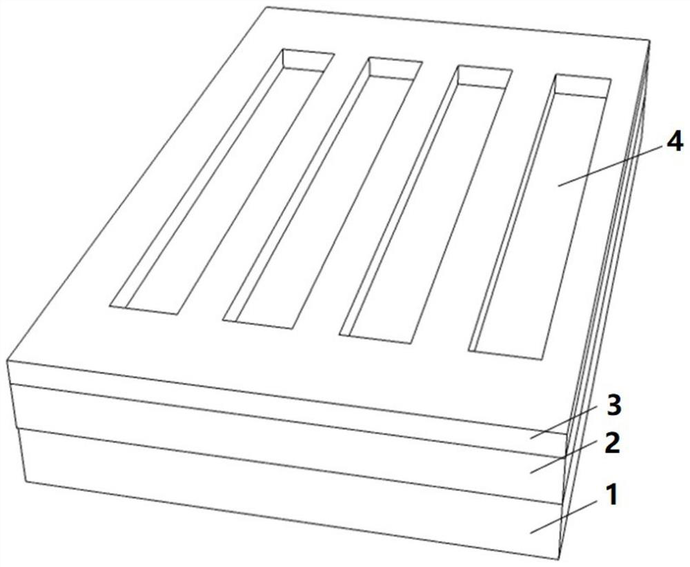
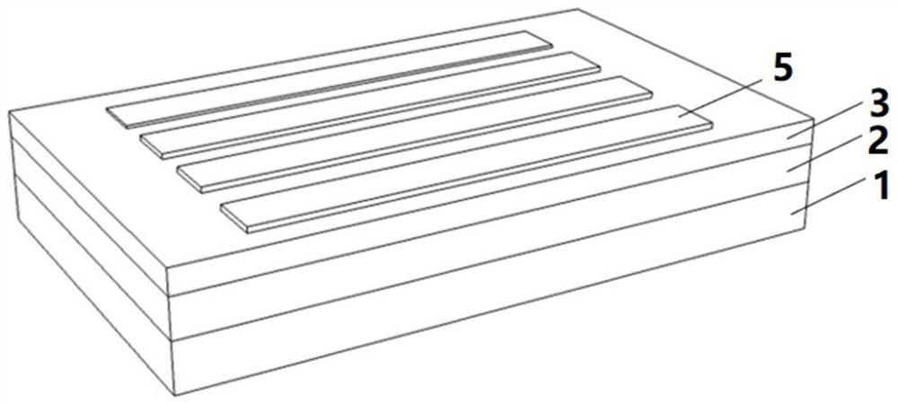
[0041] Such as Figure 1-4 As shown, a method for preparing a lateral GaN-based enhanced junction field effect transistor device, the steps include:

[0042] (1) MOCVD method deposits semi-insulating GaN layer 2 and n-GaN channel layer 3 on the surface of sapphire substrate 1, as figure 1 Shown; growth method of semi-insulating GaN: trimethylgallium and NH 3 As Ga source and N source respectively, the carrier gas is H 2 or N 2 , the growth temperature is 1000-1100°C, and the growth time is 3-5h. The growth method of the n-GaN channel layer: the temperature is 950-1050°C, the silicon doping concentration is 1*10 18 cm -3, growth time 15-20min;

[0043] (2) With the method of ICP chlorine-based plasma etching, etch a plurality of grooves 4 on the n-GaN substrate, the depth of the grooves reaches the semi-insulating GaN layer and overcuts 50-100nm to ensure the is completely removed, as figure 2 shown;

[0044] (3) Use mask selection process, use MOCVD or MBE system to ...

Embodiment 2

[0047] The preparation method of the lateral GaN-based enhancement type junction field effect transistor device is basically the same as that of the first embodiment, the difference is that the p-GaN strip structure is basically flush with the surface of the n-GaN channel layer.

Embodiment 3

[0049] A method for preparing a lateral GaN-based enhanced junction field effect transistor device, the steps comprising:

[0050] (1) MOCVD method deposits semi-insulating GaN layer and n-GaN channel layer on the surface of SiC substrate, the growth method of semi-insulating GaN: trimethylgallium and NH 3 As Ga source and N source respectively, the carrier gas is H 2 or N 2 , the growth temperature is 1000-1100°C, and the growth time is 3-5h. The growth method of the n-GaN channel layer: the temperature is 950-1050°C, the silicon doping concentration is 1*10 18 cm -3 , growth time 15-20min;

[0051] (2) Using ion implantation (the energy of ions is 100-120KeV, and the implantation dose is 1*10 18 cm -3 -1x10 19 cm -3 , annealing at 800-1200 degrees for 30s-60s), injecting multiple pieces of p-GaN with a parallel structure into the n-GaN channel layer to form multiple sandwich p-n junctions;

[0052] (3) Make Ti / Al / Ni / Au30 / 150 / 50 / 150nm multilayer metal on both ends o...


PUM

PropertyMeasurementUnit
heightaaaaaaaaaa
widthaaaaaaaaaa
thicknessaaaaaaaaaa

Abstract

The invention discloses a lateral GaN-based enhanced junction field effect transistor device and a preparation method thereof. The device uses grooving + epitaxial regrowth or ion implantation to obtain a multi-piece vertical strip structure p-GaN on the n-GaN substrate, and forms multiple thin p-n junction lateral n-type channels with the n-GaN substrate. Then, through the control of channel thickness and p-type and n-type doping concentrations, the n-type channel is in a completely depleted state of the built-in electric field of the p-n junction under zero bias, that is, the device is in the off state, and a positive Only when the bias voltage can make the channel conduct, that is, the device has a positive threshold voltage. At the same time, the multi-channel ensures the high current output of the device.

Description

technical field [0001] The invention relates to an enhanced junction field effect transistor (JFET), in particular to a lateral GaN-based enhanced junction field effect transistor. Background technique [0002] As the core devices of power electronic systems such as power conversion, control circuits, and power management, power semiconductor devices are widely used in important fields such as power transmission, transportation, and consumer electronics. GaN-based field-effect transistors have broad application prospects due to their advantages such as high operating frequency, low on-resistance, high power density, and high breakdown voltage. AlGaN / GaN heterojunction high electron mobility transistor (HEMT) develops rapidly because the growth process is relatively easy to realize, while GaN-based junction field effect transistor (JFET) needs to use regrowth or ion implantation process to realize the p-n junction. The process is more complicated, so its development is relat...

Claims


Application Information

Patent Timeline
Patent Type & Authority Patents(China)
IPC IPC(8): H01L29/10H01L29/808H01L21/337
CPCH01L29/1029H01L29/66901H01L29/808
Inventor 郭慧陈敦军张荣郑有炓
Owner NANJING UNIV
Why Eureka
Try Eureka