A μled light-emitting device without electrical contact based on wavelength down-conversion

A wavelength down-conversion and electrical contact technology, applied in electrical components, semiconductor devices, circuits, etc., can solve problems such as time-consuming and unfavorable full-color μLED display devices, and achieve complex manufacturing processes and improve color conversion efficiency. , to avoid the effect of the production process

Active Publication Date: 2021-05-18
FUZHOU UNIV
View PDF2 Cites 0 Cited by
  • Summary
  • Abstract
  • Description
  • Claims
  • Application Information

AI Technical Summary

Problems solved by technology

Due to the different epitaxial processes of the red, green and blue μLED chips, it is not conducive to the development of full-color μLED display devices; in addition, this technology also requires precise alignment and bonding of the cathode and anode electrodes in the μLED chip and the driving module, so as to realize Precise electrical contact, this process takes a lot of time due to the huge amount of μLED dies that need to be picked, placed and assembled with high precision

Method used


Image

  • A μled light-emitting device without electrical contact based on wavelength down-conversion
  • A μled light-emitting device without electrical contact based on wavelength down-conversion
  • A μled light-emitting device without electrical contact based on wavelength down-conversion

Examples


Embodiment Construction

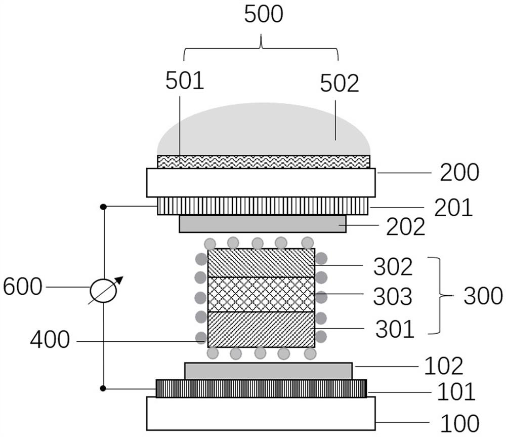
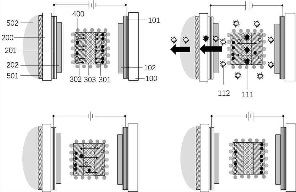
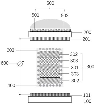
[0025] The technical solution of the present invention will be specifically described below in conjunction with the accompanying drawings.

[0026] In order to make the object, technical solution and advantages of the present invention clearer, the present invention will be further described in detail below through specific embodiments and related drawings. In the drawings, the thicknesses of layers and regions are exaggerated for clarity, but as a schematic diagram, it should not be considered as strictly reflecting the proportional relationship of geometric dimensions. Here, the referenced figures are schematic diagrams of idealized embodiments of the present invention, and embodiments of the present invention should not be construed as limited to the particular shapes of regions shown in the figures, but to include resulting shapes, such as manufacturing-induced deviations. In this embodiment, they are all represented by rectangles or circles, and the representations in the...


PUM

PropertyMeasurementUnit
thicknessaaaaaaaaaa
thicknessaaaaaaaaaa
sizeaaaaaaaaaa

Abstract

The invention relates to a micro LED light-emitting device based on wavelength down-conversion without electrical contact. Including μLED crystal grains, wavelength down-conversion luminescent layer, upper and lower driving electrodes, insulators, optical microstructures and control modules, the upper and lower driving electrodes and the μLED crystal grains have no direct electrical contact, and the control modules are respectively being electrically connected to the upper and lower driving electrodes, providing alternating driving signals for the upper and lower driving electrodes to form a driving electric field, and the driving electric field controls electrons and holes of the μLED grain to recombine and emit a first light source, converted into a second light source through the wavelength down-converting light-emitting layer. The driving electrode in the non-electrical contact μLED light-emitting device based on wavelength down-conversion proposed by the present invention has no electrical contact with the p-type semiconductor layer and n-type semiconductor layer in the μLED crystal grain, which can avoid the complicated manufacturing process of the chip in the μLED light-emitting device , and the bonding and mass transfer process of μLED chips and driver chips, effectively reducing the production cycle and cost of μLED devices.

Description

technical field [0001] The invention relates to the field of integrated semiconductor display, in particular to a non-electric contact μLED light-emitting device based on wavelength down-conversion. Background technique [0002] In the field of flat panel display technology, μLED display is to miniaturize traditional LEDs to form micron-scale LED arrays to achieve ultra-high-density pixel resolution. Compared with OLED and LCD displays, μLED has many advantages, the most notable ones are its low power consumption, high brightness, ultra-high definition, high color saturation, fast response, long life and higher work efficiency; In addition, due to the characteristics of high density, small size, and super multi-pixels, μLED will become the leader of the third-generation display technology featuring high fidelity, interactive and personalized display. Therefore, μLED display is a revolutionary new display technology that is expected to replace almost all applications of LCD ...

Claims


Application Information

Patent Timeline
Patent Type & Authority Patents(China)
IPC IPC(8): H01L33/06H01L33/10H01L33/38
CPCH01L33/06H01L33/38H01L33/10H01L33/502H01L33/62H01L33/58H01L33/46H01L33/08H01L33/0004H01L33/60
Inventor 张永爱翁徐阳郭太良周雄图吴朝兴林志贤孙磊严群
Owner FUZHOU UNIV
Why Eureka
Try Eureka