Nanotube device and manufacturing method thereof

A manufacturing method and technology of nanotubes, applied in semiconductor/solid-state device manufacturing, nanotechnology, nanotechnology, etc., can solve problems such as the complexity of nanotube structure and process, achieve mass production, improve gate control capabilities, and good compatibility sexual effect

Active Publication Date: 2020-01-24
INST OF MICROELECTRONICS CHINESE ACAD OF SCI
View PDF8 Cites 1 Cited by
  • Summary
  • Abstract
  • Description
  • Claims
  • Application Information

AI Technical Summary

Problems solved by technology

However, the nanotube structure is relatively complex in terms of process realization, which reduces the difficulty of manufacturing and has good compatibility with existing processes, which is the key issue for realizing the mass production of nanotube devices.

Method used


Image

  • Nanotube device and manufacturing method thereof
  • Nanotube device and manufacturing method thereof
  • Nanotube device and manufacturing method thereof

Examples


Embodiment Construction

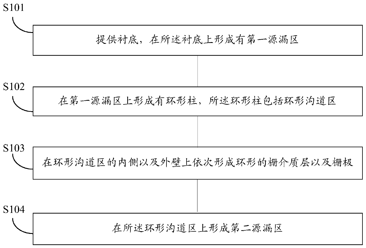
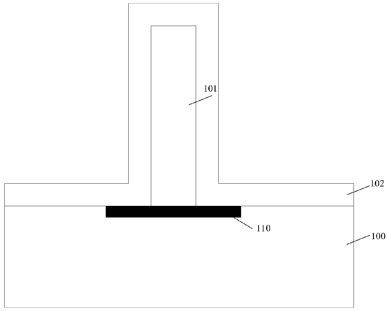
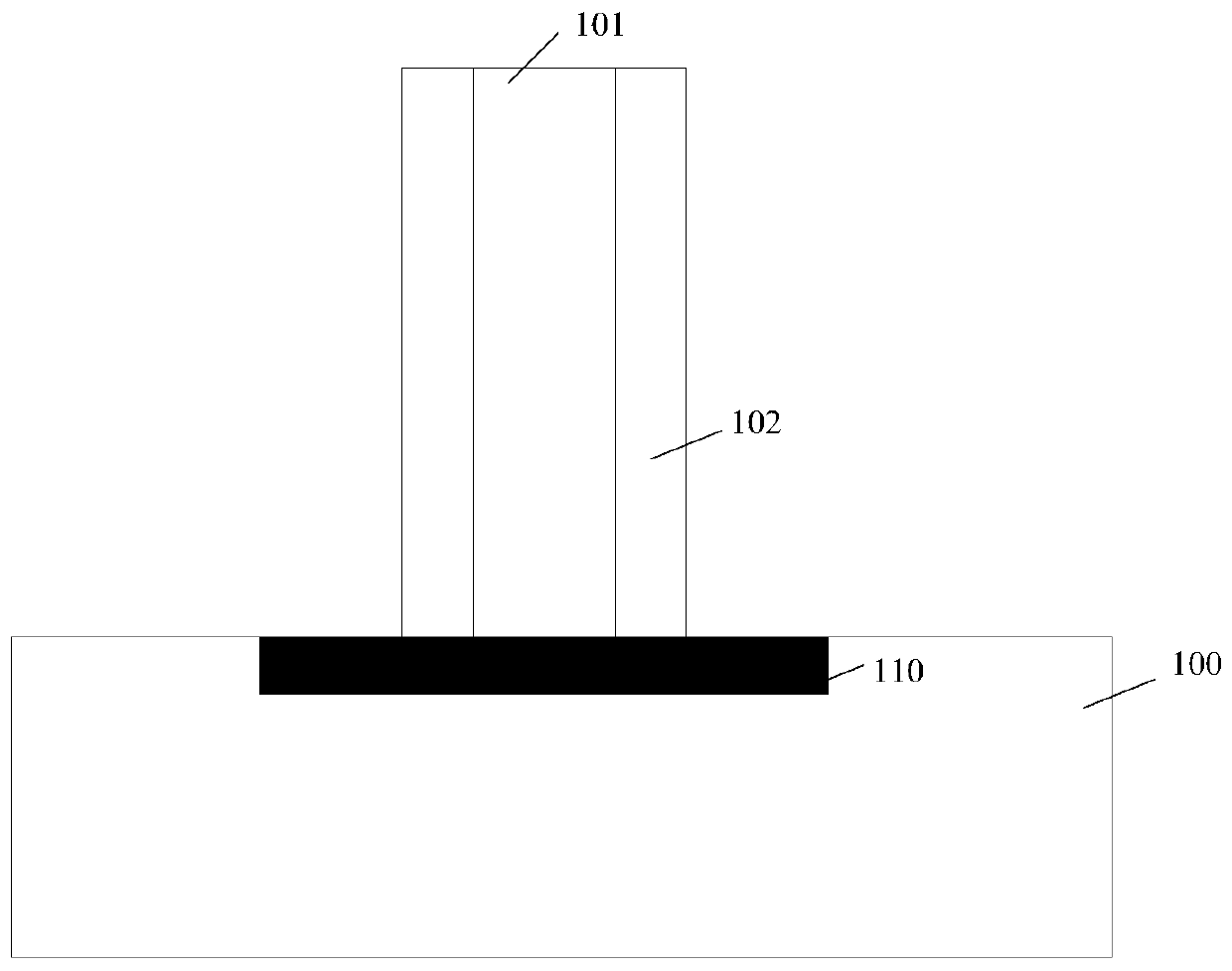
[0044] In order to make the above objects, features and advantages of the present invention more comprehensible, specific implementations of the present invention will be described in detail below in conjunction with the accompanying drawings.

[0045] In the following description, a lot of specific details are set forth in order to fully understand the present invention, but the present invention can also be implemented in other ways different from those described here, and those skilled in the art can do it without departing from the meaning of the present invention. By analogy, the present invention is therefore not limited to the specific examples disclosed below.

[0046] Secondly, the present invention is described in detail in combination with schematic diagrams. When describing the embodiments of the present invention in detail, for the convenience of explanation, the cross-sectional view showing the device structure will not be partially enlarged according to the gener...


PUM


Abstract

The invention provides a nanotube device and a manufacturing method thereof. The manufacturing method comprises the following steps: providing a substrate in which a first source-drain region is formed; forming an annular column on the first source-drain region, the annular column comprising an annular channel region; sequentially forming annular gate dielectric layers and gates on the inner walland the outer wall of the annular channel region; and forming a second source-drain region on the annular channel region. In the method, gates are formed on the inner side wall and the outer side wallof a nanotube, so that a source region-gate-drain region nanotube device structure is formed on the inner and outer sides of the nanotube in the longitudinal direction, the gate area is increased, the gate control capability is improved, and the device has higher driving current. Moreover, the manufacturing difficulty is low, the compatibility with the existing process is good, and mass production of the nanotube device is facilitated.

Description

technical field [0001] The invention relates to the field of semiconductor devices and its manufacture, in particular to a nanotube device and its manufacturing method. Background technique [0002] With the continuous development of integrated circuit manufacturing technology, the critical dimensions of semiconductor devices, especially field-effect transistors (MOSFETs), have been continuously reduced, even down to 7nm and below nodes, and the short-channel effect of devices has become more and more significant. Traditional planar The device has been unable to meet the requirements of the device in terms of performance and integration. [0003] At present, a three-dimensional device structure is proposed, which improves the gate control ability by increasing the number of gates and the channel area, so that the device has a stronger drive current, which can effectively suppress the short channel effect. Nanotube device is a three-dimensional device with larger channel are...

Claims


Application Information

Patent Timeline
Patent Type & Authority Applications(China)
IPC IPC(8): H01L29/786H01L29/775H01L21/336B82Y40/00B82Y30/00B82Y10/00
CPCH01L29/66742H01L29/78618H01L29/78642H01L29/78696H01L29/775B82Y10/00B82Y30/00B82Y40/00
Inventor 刘金彪王桂磊李俊峰
Owner INST OF MICROELECTRONICS CHINESE ACAD OF SCI
Why Eureka
Try Eureka