

Avalanche photo diode (APD) bias voltage adjustment circuit based on negative voltage adjustment
An avalanche optoelectronics and bias voltage adjustment technology, applied in the direction of adjusting electrical variables, control/regulation systems, instruments, etc., can solve the problems of single pixel adjustment, low voltage stability, large area, etc., and increase the common mode Input range, enhanced sensitivity, small area effect
- Summary
- Abstract
- Description
- Claims
- Application Information
AI Technical Summary
Problems solved by technology
Method used
Image

Examples
Embodiment Construction
[0034] The present invention will be described in detail below in conjunction with the accompanying drawings and specific embodiments.
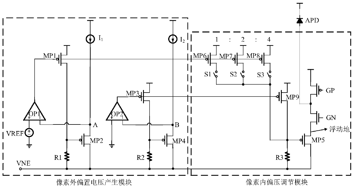
[0035] The present invention proposes an avalanche photodiode bias voltage regulation circuit based on negative voltage regulation, which includes a pixel external bias voltage generation module and a pixel internal bias voltage regulation module, such as figure 1As shown, the pixel external bias voltage generation module includes a first operational amplifier OP1, a second operational amplifier OP2, a first PMOS transistor MP1, a second PMOS transistor MP2, a third PMOS transistor MP3, a fourth PMOS transistor MP4, a first resistor R1, second resistor R2, first current source I 1 and the second current source I 2 , the non-inverting input of the first operational amplifier OP1 is connected to the reference voltage VREF, and its inverting input is connected to the source of the second PMOS transistor MP2 and the first current source I 1 , i...
PUM
 Abstract
Description
Claims
Application Information