

Dielectric film and preparation method thereof
A technology of dielectric film and dielectric constant, applied in circuits, capacitors, electrical components, etc., can solve the problems of doping, limited improvement space, etc., to improve the breakdown electric field, improve energy storage characteristics, and improve energy storage density. Effect
- Summary
- Abstract
- Description
- Claims
- Application Information
AI Technical Summary
Problems solved by technology
Method used
Image

Examples
preparation example Construction
[0026] A method for preparing a double-layer dielectric energy storage film, comprising the following steps:
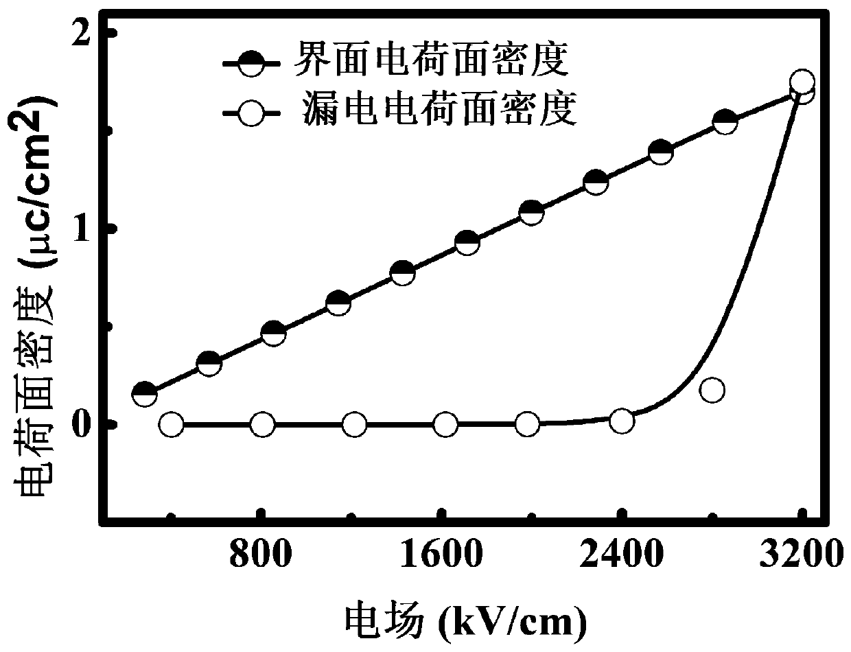
[0027] Step 1: Use the interface charge accumulation model to pre-screen the material, using the following formula
[0028]
[0029] Among them, ε 0 , ε 1 and ε 2 are the vacuum permittivity, the permittivity of raw material 1 and the permittivity of raw material 2, respectively, d 1 and d 2 are the thickness of raw material 1 and raw material 2 respectively, γ 1 and gamma 2 are the conductivity of raw material 1 and raw material 2, respectively, and u is the applied voltage of the double-layer dielectric material. Through this formula, the surface density σi of the leakage charge that can be accommodated at the interface can be calculated, and the specific value can be obtained.
[0030] Step 2: Select two materials with relatively good energy storage performance, but with differences in dielectric constant and conductivity, namely material 1 and material 2...
Embodiment 1
[0038] Implementation Example 1Na 0.5 Bi 3.25 La 1.25 Ti 4 o 15 / BaBi 3.4 La 0.6 Ti 4 o 15 Double layer dielectric energy storage film
[0039] Adopt following raw material (its purity is analytically pure, more than 99.9% of purity), utilize interface charge accumulation model; Use glue homogenizer and rapid annealing furnace to prepare Na 0.5 Bi 3.25 La 1.25 Ti 4 o 15 / BaBi 3.4 La 0.6 Ti 4 o 15 Double layer dielectric energy storage film.
[0040] The following is the preparation of a double-layer dielectric energy storage thin film with high energy storage performance Na 0.5 Bi 3.25 La 1.25 Ti 4 o 15 / BaBi 3.4 La 0.6 Ti 4 o 15 specific steps.
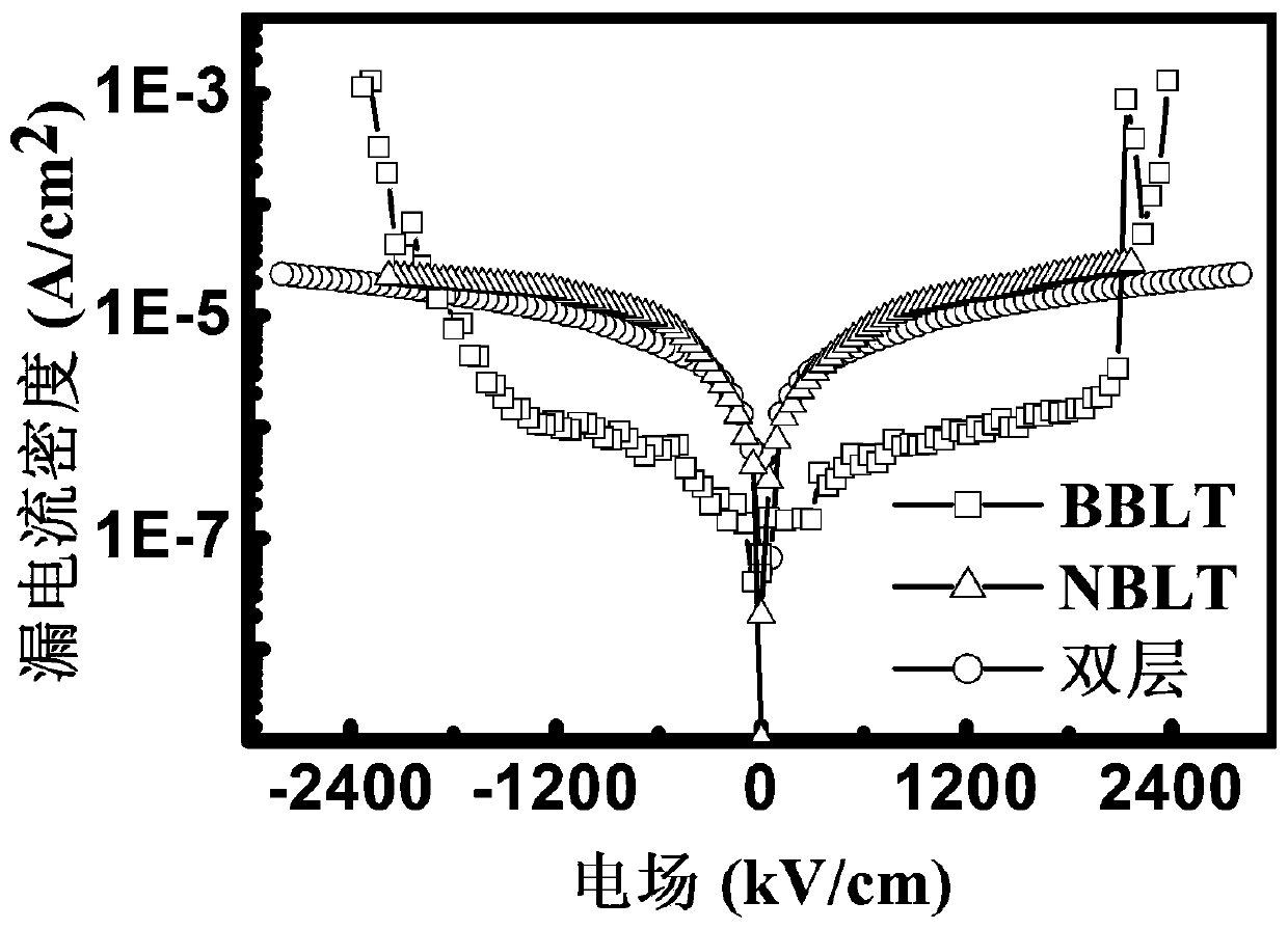
[0041] 1.1): Using the interface charge accumulation model to bring in the dielectric constant and conductivity of the original material, the relatively superior thickness ratio of the two materials is 19:16, and the surface density of the leakage charge that the interface can accommodate is obtained.
[00...
Embodiment 2
[0049] Implementation Example 2Na 0.5 Bi 3 La 1.5 Ti 4 o 15 / BaBi 3.1 La 0.9 Ti 4 o 15 Double layer dielectric energy storage film
[0050] Adopt following raw material (its purity is analytically pure, more than 99.9% of purity), utilize interface charge accumulation model; Use glue homogenizer and rapid annealing furnace to prepare Na 0.5 Bi 3 La 1.5 Ti 4 o 15 / BaBi 3.1 La 0.9 Ti 4 o 15 Double layer dielectric energy storage film.
[0051] The following is the preparation of a double-layer dielectric energy storage thin film with high energy storage performance Na 0.5 Bi 3 La 1.5 Ti 4 o 15 / BaBi 3.1 La 0.9 Ti 4 o 15 specific steps.
[0052] 1.1): Using the interface charge accumulation model, where Na 0.5 Bi 3 La 1.5 Ti 4 o 15 and BaBi 3.1 La 0.9 Ti 4 o 15 The dielectric constants are 352 and 408, respectively, and the conductivity is based on the formula γ=J / E. The conductivity under different electric fields is obtained from the leakage t...
PUM
 Abstract
Description
Claims
Application Information