Barium titanate-based superparaelectric film as well as low-temperature preparation method and application thereof

A barium titanate and paraelectric technology, which is applied in the field of barium titanate-based superparaelectric film and medium and low temperature preparation, can solve the problems of low energy density of recyclable capacitors, low dielectric constant of capacitor density, restricting the development of thin film transistors, etc. Effects of frequency stability, excellent energy storage characteristics, and small residual polarization

Active Publication Date: 2020-12-29
欧阳俊
View PDF7 Cites 3 Cited by
  • Summary
  • Abstract
  • Description
  • Claims
  • Application Information

AI Technical Summary

Problems solved by technology

High fabrication temperature will not only increase additional thermal budget, process flow and cost expenditure, but also bring great challenges to the compatibility of dielectric capacitors with CMOS-Si technology
In addition, the high temperature makes the crystallization size (grain size) larger, causing the ferroelectric capacitor to display a nearly square hysteresis dielectric response ("hysteresis loop") under an external electric field, and its recyclable capacitance has low energy density and low charge and discharge efficiency. Poor, it is difficult to integrate with existing electric energy storage and conversion technologies, and in severe cases, it will lead to device failure
Moreover, with the development of integrated circuits, in the practical application of thin film transistors, the dielectric layer materials have problems such as high preparation temperature, capacitance density and low dielectric constant, which seriously restrict the development of thin film transistors.

Method used


Image

  • Barium titanate-based superparaelectric film as well as low-temperature preparation method and application thereof
  • Barium titanate-based superparaelectric film as well as low-temperature preparation method and application thereof
  • Barium titanate-based superparaelectric film as well as low-temperature preparation method and application thereof

Examples


preparation example Construction

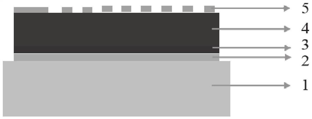
[0030] In the first aspect, the present invention provides a method for preparing a barium titanate-based superparaelectric film at a medium and low temperature, comprising the following steps:

[0031] A buffer layer of lanthanum nickelate and a base film of barium titanate are sequentially sputtered on a silicon substrate with a bottom electrode, and the deposition temperature is 25-150° C. to obtain the finished product.

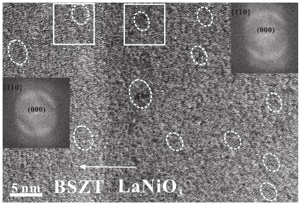
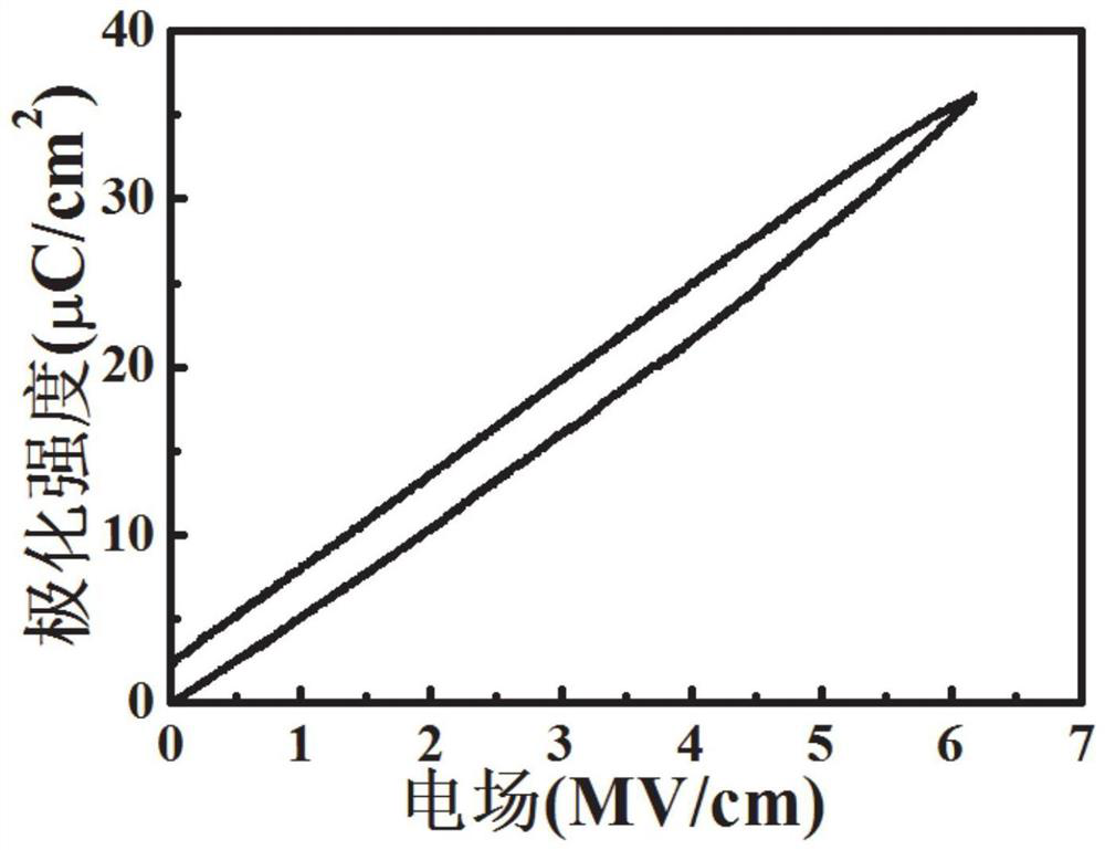
[0032] Preliminary studies have found that lanthanum nickelate can effectively reduce the crystallization temperature of the sputtered barium titanate-based film. When the sputtering temperature in the above steps is 200°C or above, the barium titanate base film will form columnar nano-grains that run through the thickness of the film, thereby presenting a ferroelectric state, making the withstand voltage (breakdown) of the barium titanate base film Voltage) decreases and remnant polarization increases, corresponding to lower recoverable energy storage de...

Embodiment 1

[0055] (a) Treatment of the substrate

[0056] Semiconductor Si / SiO 2 As the substrate, put the substrate into the sample tray, and finally put the sample tray into the sample tray rack of the vacuum coating chamber;

[0057] Vacuuming: close the vacuum chamber, evacuate, and make the air pressure in the chamber to 2×10 -4 Pa;

[0058] Heating: Ar gas is introduced into the chamber, and then the substrate is heated until the temperature rises to 300°C, and then the temperature is kept stable.

[0059] (b) Preparation of the bottom electrode

[0060] Titanium and platinum metals were used as sputtering targets, and the bottom electrode was deposited by radio frequency magnetron sputtering. The sputtering pressure is adjusted to 0.3Pa, the sputtering power is 55W, and the Si / SiO 2 Titanium and platinum are sequentially deposited on the substrate, and the total thickness of the bottom electrode is about 150nm.

[0061] (c) Preparation of buffer layer

[0062] Using lanthan...

Embodiment 2

[0071] The difference between this embodiment and Embodiment 1 is that in step (d), the perovskite oxide barium titanate ceramic is used as the sputtering target, the sputtering pressure is 1.2Pa, and the sputtering power is 100W barium titanate-based film Thickness is 350nm, other steps and parameter are identical with specific embodiment 1.


PUM

PropertyMeasurementUnit
thicknessaaaaaaaaaa
thicknessaaaaaaaaaa
thicknessaaaaaaaaaa

Abstract

The invention discloses a barium titanate-based superparaelectric film material, a method for integrally preparing a barium titanate-based superparaelectric film on a silicon substrate at medium and low temperatures and application of the barium titanate-based superparaelectric film material. The method comprises the steps that under the condition of room temperature (without heating) or 150 DEG C, a buffer layer and a barium titanate base film are sequentially subjected to magnetron sputtering on the surface of a platinum-titanium-plated base body from bottom to top, a top electrode is subjected to magnetron sputtering on the surface of the barium titanate base film, and the buffer layer is made of conductive oxide lanthanum nickelate which can be matched with barium titanate base lattices and is of a perovskite structure; the sputtering mode is a continuous sputtering mode of the lanthanum nickelate buffer layer and the barium titanate base film. According to the invention, the temperature for preparing the barium titanate-based membrane material can be reduced to room temperature or 150 DEG C, and the barium titanate-based membrane material has a nano polar region with good dispersion, high energy storage density and high energy storage efficiency, and high energy storage characteristics are not changed along with the increase of thickness. Moreover, by reducing the thickness of the superparaelectric film layer, the capacitance density and the dielectric constant are increased, and the requirement of a thin film transistor for the high dielectric constant of the dielectric layer is met.

Description

technical field [0001] The invention relates to the technical field of electronic material development and thin film material preparation, in particular to a barium titanate-based superparaelectric film and its medium and low temperature preparation method and application. Background technique [0002] The information disclosed in this background section is only intended to increase the understanding of the general background of the present invention, and is not necessarily taken as an acknowledgment or any form of suggestion that the information constitutes the prior art already known to those skilled in the art. [0003] In recent years, with the rapid development of electronic devices such as capacitors, power tuning devices, pulsed power systems, and thin-film transistors, materials and devices with high capacitance density, high dielectric constant, high energy storage density, and high energy storage efficiency are of great interest. It is one of the frontiers and hots...

Claims


Application Information

Patent Timeline
Patent Type & Authority Applications(China)
IPC IPC(8): H01L21/02
CPCH01L21/02112H01L21/02172H01L21/02304H01L21/0226Y02E60/13
Inventor 欧阳俊王坤赵玉垚
Owner 欧阳俊
Why Eureka
Try Eureka