Lead-free ceramic dielectric with high energy storage density and high energy storage efficiency and preparation method thereof

A high energy storage density, ceramic dielectric technology, applied in chemical instruments and methods, ceramic molding machines, ceramic layered products, etc., can solve the limitations of miniaturization, integration and high performance of lead-free electronic components, breakdown The electric field strength and the maximum polarization strength are difficult to improve at the same time, and the energy storage efficiency is low, so as to achieve the effect of simple and convenient preparation method, high volatility and excellent performance

Active Publication Date: 2021-02-09
TONGJI UNIV
View PDF6 Cites 0 Cited by
  • Summary
  • Abstract
  • Description
  • Claims
  • Application Information

AI Technical Summary

Problems solved by technology

However, the breakdown electric field strength and maximum polarization strength of lead-free ceramic dielectrics are often difficult to increase simultaneously, resulting in the low energy storage density of

Method used


Image

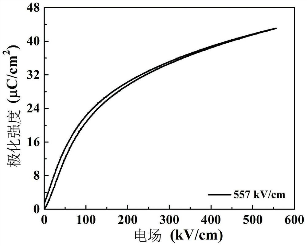
  • Lead-free ceramic dielectric with high energy storage density and high energy storage efficiency and preparation method thereof
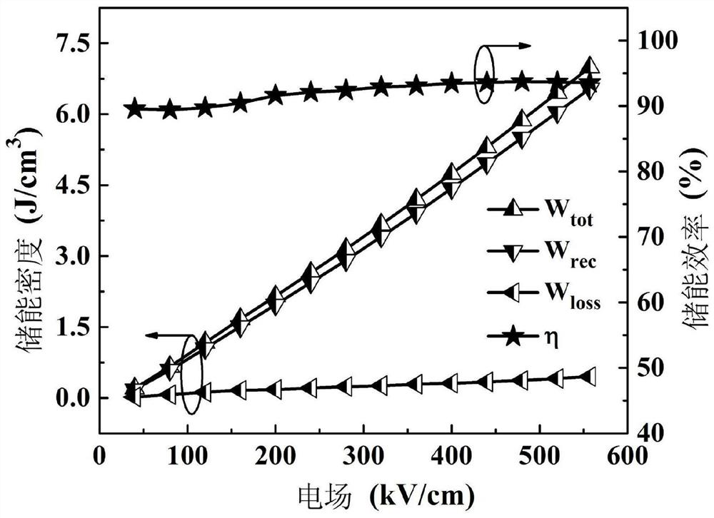
  • Lead-free ceramic dielectric with high energy storage density and high energy storage efficiency and preparation method thereof
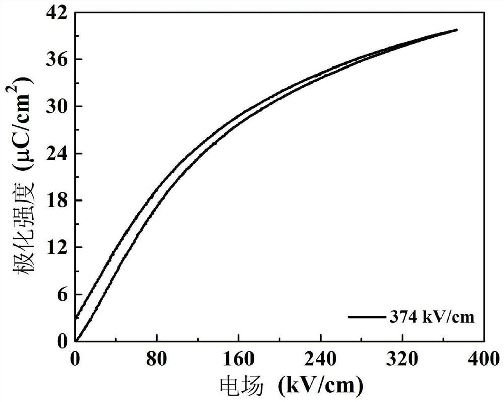
  • Lead-free ceramic dielectric with high energy storage density and high energy storage efficiency and preparation method thereof

Examples


Example Embodiment

[0066]

[0067] A preparation method of a lead-free ceramic dielectric with high energy storage density and high energy storage efficiency (hereinafter referred to as ceramic dielectric):

[0068] Step S1, according to the chemical formula 0.80Bi 0.5 Na 0.5 TiO 3 -0.20SrNb 0.5 Al 0.5 o 3 (hereinafter referred to as BNTSNA) weighed 14.3964g Bi 2 o 3 , 3.2484g Na 2 CO, 4.5612g SrCO 3 , 9.9714g TiO 2 , 0.7797g Al 2 o 3 and 2.0428gNb 2 o 5 Prepare the outer dielectric material as a raw material, and then according to the chemical formula 0.94Bi 0.55 Na 0.45 TiO 3 -0.06BaTiO 3 (hereinafter referred to as BNBT) weighed 40.9673g Bi 2 o 3 , 7.5632g Na 2 CO 3 , 4.0271g BaCO 3 , 27.4423g TiO 2 Prepare the inner layer dielectric material as a raw material;

[0069] Step S2, put the raw material of the outer layer dielectric material and the raw material of the inner layer dielectric material into two ball milling tanks respectively, then add absolute ethanol and ...

Example Embodiment

[0079]

[0080] A preparation method of a lead-free ceramic dielectric with high energy storage density and energy storage efficiency:

[0081] Step S1, according to the chemical formula 0.94Bi 0.55 Na 0.45 TiO 3 -0.06BaTiO 3 (hereinafter referred to as BNBT) weighed 40.9673g Bi 2 o 3 , 7.5632g Na 2 CO 3 , 4.0271g BaCO 3 , 27.4423g TiO 2 Prepare the outer dielectric material as a raw material, and then according to the chemical formula 0.80Bi 0.5 Na 0.5 TiO 3 -0.20SrNb 0.5 al 0.5 o 3 (hereinafter referred to as BNTSNA) weighed 14.3964gBi 2 o 3 , 3.2484g Na 2 CO, 4.5612g SrCO 3 , 9.9714g TiO 2 , 0.7797g Al 2 o 3 and 2.0428g Nb 2 o 5 Prepare the inner layer dielectric material as a raw material;

[0082] Step S2, put the raw material of the outer layer dielectric material and the raw material of the inner layer dielectric material into two ball milling tanks respectively, then add absolute ethanol and ZrO in the two ball milling tanks respectively 2 balls...

Example Embodiment

[0092]

[0093] A preparation method of a lead-free ceramic dielectric with high energy storage density and energy storage efficiency:

[0094] Step S1, according to the chemical formula 0.80Bi 0.5 Na 0.5 TiO 3 -0.20SrNb 0.5 al 0.5 o 3 (hereinafter referred to as BNTSNA) weighed 14.3964g Bi 2 o 3 , 3.2484g Na 2 CO, 4.5612g SrCO 3 , 9.9714g TiO 2 , 0.7797g Al 2 o 3 and 2.0428gNb 2 o 5 Prepare the outer dielectric material as a raw material, and then according to the chemical formula 0.75Bi 0.52 Na 0.48 TiO 3 -0.25SrTiO 3 (hereinafter referred to as BNST) weighed 15.9842g Bi 2 o 3 , 3.3293g Na 2 CO 3 , 6.4927g SrCO 3 , 14.1939g TiO 2 Prepare the inner layer dielectric material as a raw material;

[0095] Step S2, put the raw material of the outer layer dielectric material and the raw material of the inner layer dielectric material into two ball milling tanks respectively, then add absolute ethanol and ZrO in the two ball milling tanks respectively 2 bal...


PUM

PropertyMeasurementUnit
Electric field strengthaaaaaaaaaa
Energy storage densityaaaaaaaaaa
Electric field strengthaaaaaaaaaa

Abstract

The invention belongs to the technical field of energy storage ceramic dielectric materials, and provides a lead-free ceramic dielectric with high energy storage density and high energy storage efficiency and a preparation method thereof. The preparation method includes the steps of synthesizing inner-layer ceramic powder and outer-layer ceramic powder through a solid-phase reaction, using the powder to further prepare ceramic slurry, and obtaining a corresponding ceramic film through a tape casting process; and pressurizing the obtained ceramic membrane under different temperature and pressure conditions, and finally conducting sintering at the high temperature of 1050-1200 DEG C to obtain the lead-free high-energy-storage-density and high-energy-storage-efficiency ceramic dielectric withthe layered sandwich structure, wherein a first dielectric layer and a third dielectric layer have high breakdown field intensity, and a second dielectric layer has high polarization intensity, or the first dielectric layer and the third dielectric layer have high polarization intensity, and the second dielectric layer has high breakdown field intensity. The material does not contain lead, is simple in preparation process, stable in preparation process, suitable for industrial batch production, excellent in pressure resistance and high in energy storage density and efficiency, and integratesexcellent properties of various materials.

Description

technical field [0001] The invention belongs to the technical field of energy storage ceramic dielectric materials, in particular to a lead-free ceramic dielectric with high energy storage density and high energy storage efficiency and a preparation method thereof. Background technique [0002] In recent years, with the rapid development of information technology, the requirements for material properties are getting higher and higher. Due to its fast charging and discharging speed, high power density, long cycle life, wide operating temperature range, and good stability, ceramic dielectric capacitors have broad applications in many fields such as new energy electric vehicles, laser weapons, smart grids, and electromagnetic guns. Application prospects. With restrictions on lead-containing materials in electronic components around the world, finding and developing lead-free ceramic dielectric capacitors that can replace lead-based materials has become a current research hotsp...

Claims


Application Information

Patent Timeline
IPC IPC(8): C04B35/475C04B35/622C04B35/626B28B1/29B28B11/00B32B9/00B32B9/04B32B18/00
CPCC04B35/475C04B35/622C04B35/6264C04B35/6261C04B35/62655B28B1/29B28B11/003B32B9/005B32B9/04B32B18/00C04B2235/3298C04B2235/3215C04B2235/3201C04B2235/3213C04B2235/3217C04B2235/3232C04B2235/3251C04B2235/3236C04B2235/60B32B2250/40B32B2307/204
Inventor 翟继卫闫非沈波
Owner TONGJI UNIV
Why Eureka
Try Eureka