
Enhanced GaNHEMT integrated structure and preparation method thereof

An enhanced, mesa-structured technology, used in semiconductor/solid-state device manufacturing, electrical components, circuits, etc., to solve problems such as device performance degradation, increased dynamic on-resistance, and very high requirements for etching accuracy, thickness, and surface roughness. , to reduce the difficulty of the preparation process, achieve normally-off characteristics, and reduce the effect of current collapse

Active Publication Date: 2020-02-14
XI AN JIAOTONG UNIV
View PDF7 Cites 0 Cited by
  • Summary
  • Abstract
  • Description
  • Claims
  • Application Information

AI Technical Summary

Problems solved by technology

At this stage, the commonly used technical means to obtain enhancement devices are p-GaN gate FET and insulated gate (MIS) FET, and the process steps have p-GaN gate or Al x Ga 1-x Etching of the N barrier layer has very high requirements on etching precision, thickness, surface roughness, etc., and etching damage will lead to a decrease in device performance and an increase in dynamic on-resistance

Method used

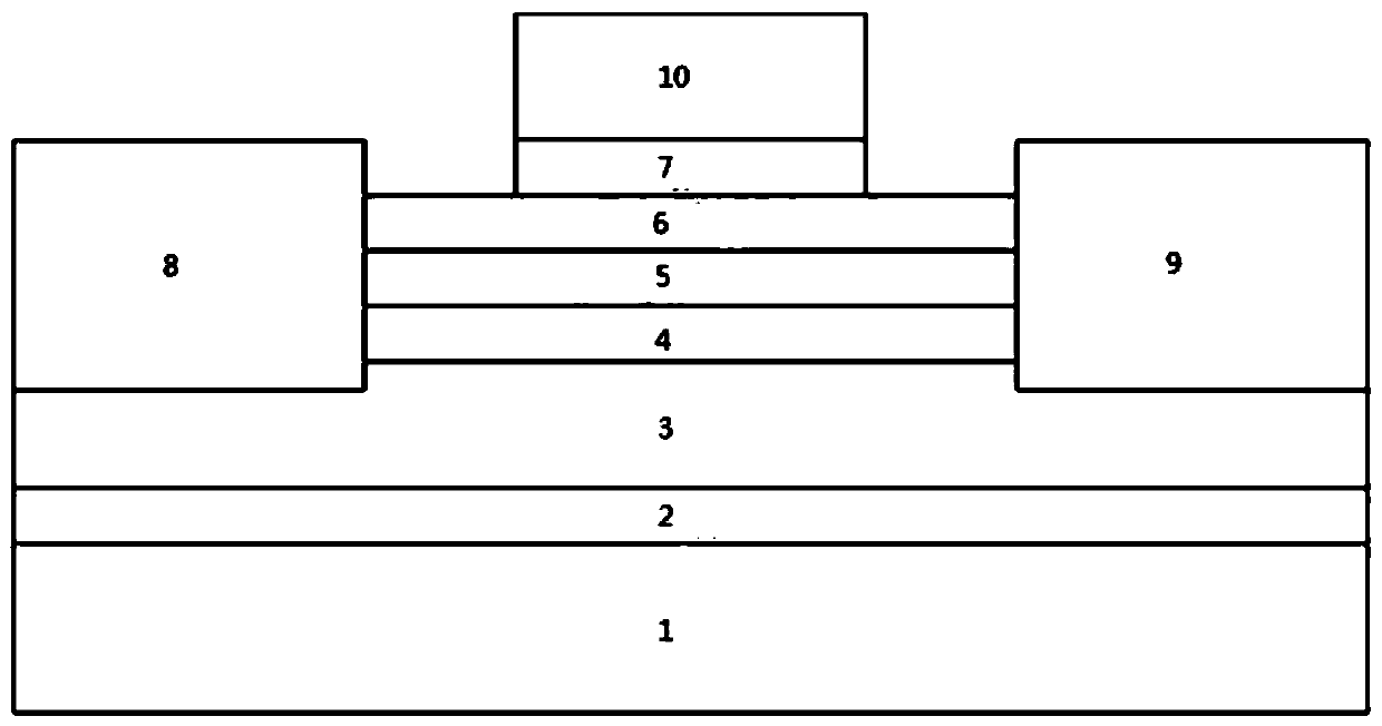

Image

  • Enhanced GaNHEMT integrated structure and preparation method thereof
  • Enhanced GaNHEMT integrated structure and preparation method thereof

Examples


Embodiment 1

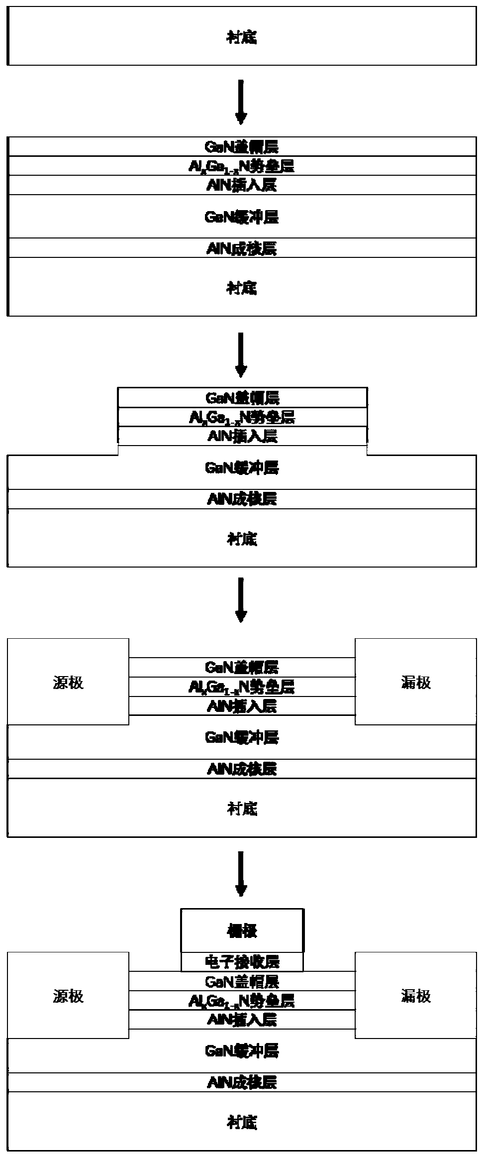
[0049] A method for preparing an enhanced GaNHEMT integrated structure according to an embodiment of the present invention includes the following steps:

[0050] 1) Use the substrate standard cleaning process to carry out inorganic and organic cleaning on the Si-based substrate successively, and dry it with nitrogen gas for later use.

[0051] 2) AlN nucleation layer, GaN buffer layer, AlN insertion layer, Al x Ga 1-x N barrier layer, GaN capping layer.

[0052] 3) Clean the GaN epitaxial material grown in step 2) with the standard process, blow it dry with nitrogen, spin-coat a layer of AZ5214 photoresist on the surface, bake the sample with spin-coated photoresist at 95°C for 90 seconds, and use the design A good mask plate is exposed to ultraviolet lithography for 4s, and developed for 30s to remove the exposed photoresist, leaving the pattern of the mesa area. Harden the film on a hot plate at 120°C for 120s.

[0053] 4) Place the photoetched sample in the sample chamb...

Embodiment 2

[0058] A method for preparing an enhanced GaNHEMT integrated structure according to an embodiment of the present invention includes the following steps:

[0059] 1) Use the substrate standard cleaning process to perform inorganic and organic cleaning on the GaN substrate successively, and dry it with nitrogen gas for later use.

[0060] 2) AlN nucleation layer, GaN buffer layer, AlN insertion layer, Al x Ga 1-x N barrier layer, GaN capping layer.

[0061] 3) Clean the grown GaN epitaxial material with standard process, dry it with nitrogen gas, spin-coat a layer of KXN5735-LO photoresist on the surface of the sample, and bake the GaN sample with spin-coated photoresist at 95°C for 90 seconds , use the designed mask to expose to UV lithography for 2s, develop for 25s to remove the exposed photoresist, and leave the pattern of the etched area. Harden the remaining photoresist at 120°C for 120s.

[0062] 4) Place the photolithographic sample in the sample chamber of the ion b...

Embodiment 3

[0067] In the embodiment of the present invention, the difference from embodiment 1 is only:

[0068] The substrate material is diamond, with a size of 1 to 12 inches; the material of the electron receiving layer is V 2 o 5 , the thickness of the AlN nucleation layer is 2-5 nm, the thickness of the GaN buffer layer is 1-5 μm, the thickness of the AlN insertion layer is 0-5 nm, the Al x Ga 1-x The thickness of the N barrier layer is 2-30nm, and the thickness of the GaN capping layer is 0-2nm.

[0069]The materials of the source electrode and the drain electrode are Ti, Al and Ni, and the materials of the gate electrode are Ni, Au and Pt.

[0070] Deposit materials on the GaN capping layer and GaN buffer layer of the mesa structure to form source and drain electrodes; among them, the ohmic contact should cover part of the GaN capping layer, part of the buffer layer, and the N 2 Annealing in a mixed atmosphere with Ar, the annealing temperature is 1000°C, and the annealing ti...


PUM

PropertyMeasurementUnit
thicknessaaaaaaaaaa
thicknessaaaaaaaaaa
thicknessaaaaaaaaaa

Abstract

The invention discloses an enhanced GaNHEMT integrated structure and a preparation method thereof. The enhanced GaNHEMT integrated structure comprises a substrate. The HEMT integrated structure further comprises an AlN nucleating layer formed on the substrate, a GaN buffer layer is formed on the AlN nucleating layer, an AlN insertion layer formed on the GaN buffer layer, an AlxGa<1-x>N barrier layer formed on the AlN insertion layer, a GaN cap layer formed on the AlxGa<1-x>N barrier layer, and an electron receiving layer formed on the GaN cap layer, wherein the work function of the electron receiving layer is greater than the work function of the AlxGa<1-x>N barrier layer, and electrons can be transferred to the electron receiving layer from a two-dimensional channel of the AlxGa<1-x>N / GaNinterface. According to the enhanced GaNHEMT integrated structure, the work function difference between the electron receiving layer and the barrier layer is utilized to generate a wide space chargeregion, so that electrons are enabled to flow into the electron receiving layer from a two-dimensional electron gas of the GaN / AlGaN heterogeneous interface, and the channel below the gate is depletedto obtain enhanced device characteristics.

Description

technical field [0001] The invention belongs to the technical field of semiconductor devices, in particular to an enhanced GaNHEMT integrated structure and a preparation method thereof. Background technique [0002] The first generation of Si and Ge semiconductors brought mankind into the information age, and at the same time drove the intelligence and informatization of electronic systems. The second-generation semiconductors (GaAs, InP, MCT, etc.) have brought us optoelectronic devices, power electronic devices, radio frequency electronic devices, and space radiation-resistant devices, which have triggered revolutions in information fields such as wireless communications and optical communications. The third-generation semiconductor GaN has excellent semiconductor characteristics such as wide bandgap, high breakdown, and high frequency; compared with Si-based semiconductors, the breakdown field strength of GaN materials is more than 10 times higher, and the Baliga figure o...

Claims


Application Information

Patent Timeline
Patent Type & Authority Applications(China)
IPC IPC(8): H01L29/06H01L29/778H01L21/335
CPCH01L29/7781H01L29/66462H01L29/0684
Inventor 王玮王宏兴问峰张明辉林芳陈根强
Owner XI AN JIAOTONG UNIV
Learn More