SRAM (Static Random Access Memory) storage unit circuit capable of realizing high read-write stability under low voltage

A storage unit circuit and stability technology, applied in the direction of information storage, static memory, digital memory information, etc., can solve the problems of low static power consumption, etc., to improve writing ability, reduce static power consumption, and reduce write bit line leakage The effect of current

Active Publication Date: 2020-02-18
UNIV OF ELECTRONIC SCI & TECH OF CHINA
View PDF8 Cites 2 Cited by
  • Summary
  • Abstract
  • Description
  • Claims
  • Application Information

AI Technical Summary

Problems solved by technology

[0004] Aiming at the problem of lower write capability and read interference of single-ended SRAM cells under low voltage, the present invention proposes a single-ended 9-tube SRAM memory cell circuit, which can Improve reading and writing stability and have low static powe

Method used


Image

  • SRAM (Static Random Access Memory) storage unit circuit capable of realizing high read-write stability under low voltage
  • SRAM (Static Random Access Memory) storage unit circuit capable of realizing high read-write stability under low voltage
  • SRAM (Static Random Access Memory) storage unit circuit capable of realizing high read-write stability under low voltage

Examples


Embodiment Construction

[0018] The present invention will be described in detail below in conjunction with the accompanying drawings and specific embodiments.

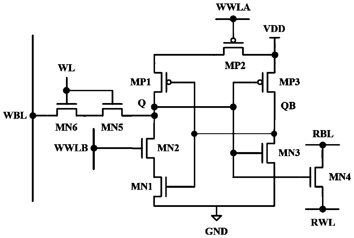
[0019] The present invention proposes a 9-tube SRAM storage unit circuit, which can improve the stability of reading and writing under low voltage and has low static power consumption, and is suitable for single-ended reading and writing array structures, such as figure 2 Shown is a schematic structural diagram of the SRAM storage unit circuit proposed by the present invention, including a first NMOS transistor MN1, a second NMOS transistor MN2, a third NMOS transistor MN3, a fourth NMOS transistor MN4, a fifth NMOS transistor MN5, and a sixth NMOS transistor MN6, the first PMOS transistor MP1, the second PMOS transistor MP2 and the third PMOS transistor MP3. The source of the first PMOS transistor MP1 is connected to the drain of the second PMOS transistor MP2, and its gate is connected to the gate of the first NMOS transistor MN1, the drai...


PUM

PropertyMeasurementUnit
Sizeaaaaaaaaaa

Abstract

An SRAM (Static Random Access Memory) storage unit circuit capable of realizing high read-write stability under low voltage is of a nine-tube structure, a grid electrode of a sixth NMOS (N-channel Metal Oxide Semiconductor) tube is connected with a grid electrode of a fifth NMOS tube and a first writing line, a drain electrode of the sixth NMOS tube is connected with a writing bit line, and a source electrode of the sixth NMOS tube is connected with a drain electrode of the fifth NMOS tube; the grid electrode of the second NMOS tube is connected with a third writing line, the drain electrode of the second NMOS tube is connected with the source electrode of the fifth NMOS tube, the drain electrode of the first PMOS tube and the grid electrodes of the third PMOS tube, the third NMOS tube andthe fourth NMOS tube, and the source electrode of the second NMOS tube is connected with the drain electrode of the first NMOS tube; the grid electrode of the second PMOS tube is connected with the second writing line, the drain electrode of the second PMOS tube is connected with the source electrode of the first PMOS tube, and the source electrode of the second PMOS tube is connected with the source electrode of the third PMOS tube and the power supply voltage; the drain electrode of the third NMOS transistor is connected with the drain electrode of the third PMOS transistor and the grid electrodes of the first NMOS transistor and the first PMOS transistor, and the source electrode of the third NMOS transistor is connected with the source electrode of the first NMOS transistor and the ground; and the drain electrode of the fourth NMOS transistor is connected with a read bit line, and the source electrode is connected with a read word line. The method can improve the writing capability of the SRAM storage unit, reduces the static power consumption of the system, does not affect the reading stability, and is especially suitable for low-voltage application.

Description

technical field [0001] The invention belongs to the technical field of integrated circuits, and relates to a 9-tube SRAM storage unit circuit, which is suitable for a single-end read-write array structure, can improve read-write stability under low voltage, and has low static power consumption. Background technique [0002] In recent years, application fields represented by wireless sensor networks and medical electronic equipment have higher and higher requirements for power consumption and performance of SoCs. Embedded static random access memory (SRAM) is one of the key components of SoCs. Reducing the power supply voltage is an effective means to ensure low power consumption of SRAM, but the reduction of the power supply voltage will bring about problems related to read and write stability. Therefore, in some applications that do not require high operating frequency, a single-ended read and write structure can be used Thereby greatly reducing system power consumption. H...

Claims


Application Information

Patent Timeline
IPC IPC(8): G11C11/419G11C11/412
CPCG11C11/419G11C11/412Y02D10/00
Inventor 贺雅娟吕嘉洵黄茂航吴晓清张波
Owner UNIV OF ELECTRONIC SCI & TECH OF CHINA
Why Eureka
Try Eureka