Shape memory embedded double-layer metal grid conducting film and preparation method thereof

A double-layer metal, embedded technology, applied in the field of flexible optoelectronics, can solve problems such as fracture and device failure, and achieve the effect of good scratch resistance, excellent corrosion resistance and oxidation resistance, and low surface roughness

Inactive Publication Date: 2020-02-25
HARBIN INST OF TECH
View PDF6 Cites 1 Cited by
  • Summary
  • Abstract
  • Description
  • Claims
  • Application Information

AI Technical Summary

Problems solved by technology

[0004] The problem solved by the present invention is that when ITO is used as a transparent elect

Method used


Image

  • Shape memory embedded double-layer metal grid conducting film and preparation method thereof
  • Shape memory embedded double-layer metal grid conducting film and preparation method thereof
  • Shape memory embedded double-layer metal grid conducting film and preparation method thereof

Examples


Example Embodiment

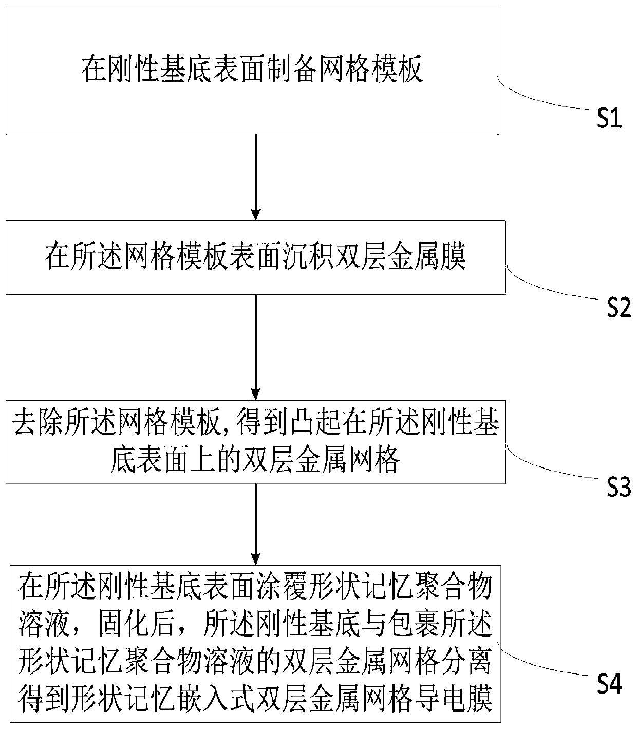
[0037] like Figure 1-3 As shown, the embodiment of the present invention provides a method for preparing a shape-memory embedded double-layer metal grid conductive film, including the following steps:

[0038] Step S1, preparing a grid template 3 on the surface of the rigid substrate 1, specifically comprising: spin-coating or spraying the polymer emulsion on the surface of the rigid substrate 1 to prepare the grid template 3;

[0039] Step S2, depositing a double-layer metal film on the surface of the grid template 3;

[0040] Step S3, removing the grid template 3 to obtain a double-layer metal grid raised on the surface of the rigid substrate 1;

[0041] Step S4, coating the shape-memory polymer 7 on the surface of the rigid substrate 1, and after curing, the rigid substrate is separated from the double-layer metal grid wrapped with the shape-memory polymer to obtain a shape-memory embedded double-layer metal mesh Lattice conductive film.

[0042] Preferably, in step S1,...

Example Embodiment

[0054] Example 1

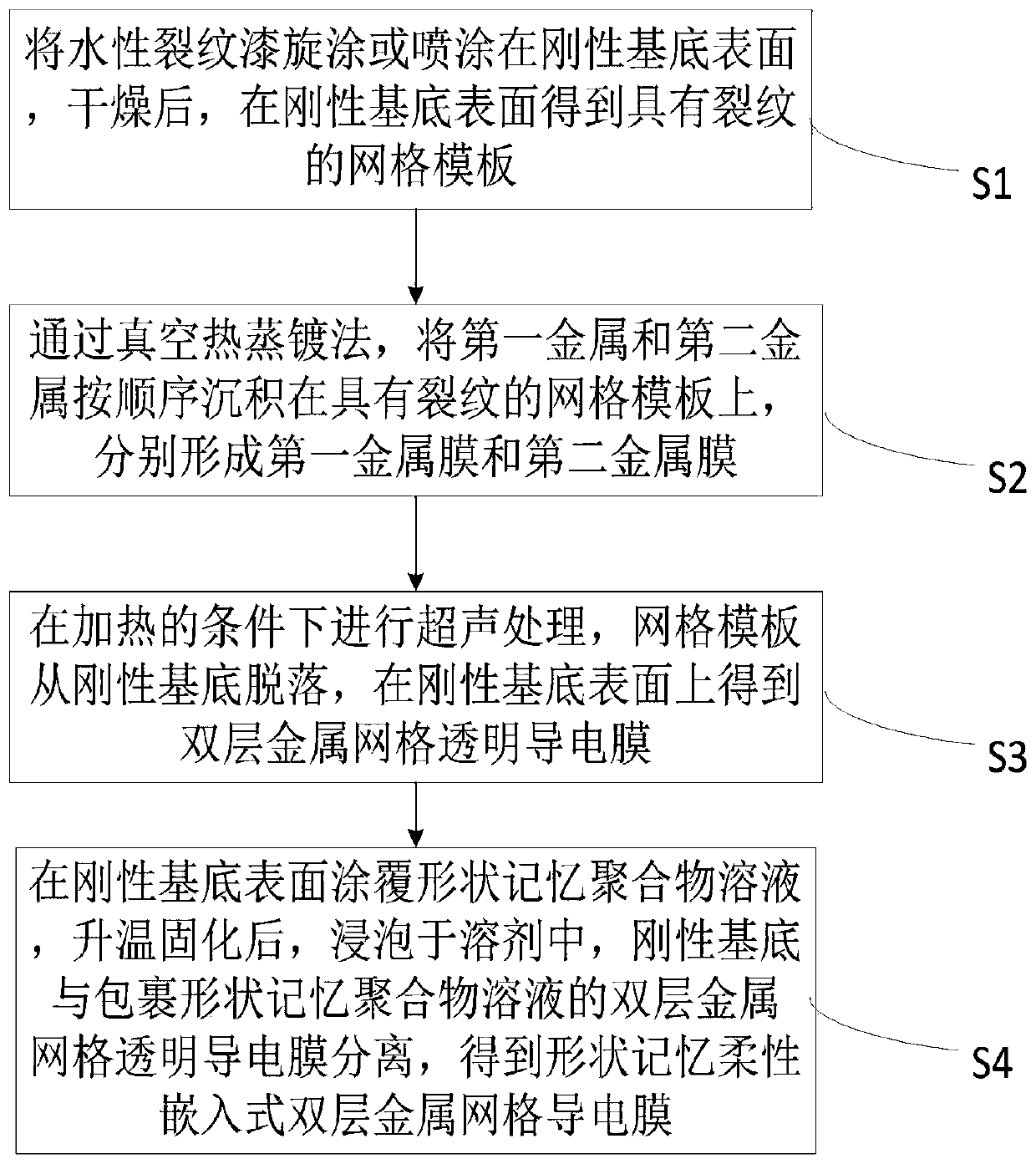
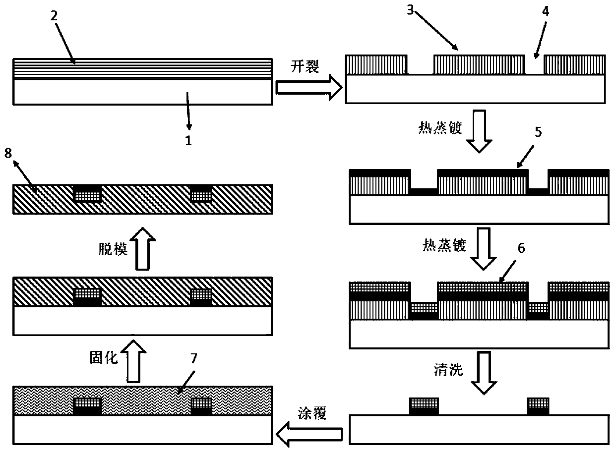
[0055] This embodiment provides a method for preparing a shape-memory embedded double-layer metal grid conductive film 8, which includes the following steps:

[0056] Step S1: preparing a grid template 3 with cracks 4;

[0057] First, prepare a water-based crackle paint emulsion with a mass fraction of 15wt%, take an appropriate amount of emulsion with a dropper and drop it on the surface of a glass sheet, prepare a layer of crackle paint 2 film by spin coating, set the speed of the glue homogenizer at 1500r / min, for 30s. The shape of the grid template 3 can be controlled by adjusting the rotational speed. The faster the rotational speed, the thinner the cracks 4 will be. On the contrary, the slower the rotational speed, the larger the width of the cracks 4 will be. Then place the glass sheet horizontally in a drying oven at 40° C. to dry for 1 min, the crack paint 2 emulsion will crack naturally, and a grid template 3 with cracks 4 will be formed on the s...

Example Embodiment

[0069] Example 2

[0070] This embodiment provides a method for preparing a shape-memory embedded double-layer metal grid conductive film 8, which includes the following steps:

[0071] Step S1: preparing a grid template 3 with cracks 4;

[0072] First prepare a water-based crackle paint emulsion with a mass fraction of 10wt%, take an appropriate amount of emulsion with a dropper and drop it on the surface of a silicon chip, and prepare a layer of crackle paint 2 film by spin coating. 30s. The shape of the grid template 3 can be controlled by adjusting the rotational speed. The faster the rotational speed, the thinner the cracks 4 will be. On the contrary, the slower the rotational speed, the larger the width of the cracks 4 will be. Then place the silicon wafer horizontally in a drying oven at 30° C. to dry for 2 minutes, and the crack paint 2 emulsion will crack naturally, forming a layer of grid template 3 with cracks 4 on the surface of the silicon wafer.

[0073] Step ...


PUM

PropertyMeasurementUnit
Thickness rangeaaaaaaaaaa
Thicknessaaaaaaaaaa
Thicknessaaaaaaaaaa

Abstract

The invention provides a shape memory embedded double-layer metal grid conducting film and a preparation method thereof, which belong to the technical field of flexible photoelectrons. The preparationmethod for the shape memory embedded double-layer metal grid conducting film comprises the following steps of: preparing a grid template on the surface of a rigid substrate, depositing a double-layermetal film on the surface of the grid template, removing the grid template to obtain a double-layer metal grid protruding on the surface of the rigid substrate, and coating the surface of the rigid substrate with a shape memory polymer, and after curing, separating the rigid substrate from the double-layer metal grid wrapping the shape memory polymer to obtain the shape memory embedded double-layer metal grid conducting film. Compared with the prior art, the shape memory embedded double-layer metal grid conducting film prepared by the invention has good scratch resistance, bending stability,corrosion resistance, oxidation resistance and shape memory performance.

Description

technical field [0001] The invention relates to the technical field of flexible optoelectronics, in particular to a shape-memory embedded double-layer metal grid conductive film and a preparation method thereof. Background technique [0002] Flexible transparent electrodes are a key part of flexible electronic devices. The most commonly used electrode material in traditional non-flexible semiconductor optoelectronic devices is ITO, and ITO is a very brittle material. When it is bent by 2% to 3%, cracks will appear and The crack will extend and greatly affect its electrical performance. Therefore, if ITO is used as a transparent electrode in a flexible electronic device, due to the existence of bending or curling application, ITO is easy to break and cause device failure. Therefore, it is inevitable and urgent to find a replacement for ITO. [0003] In summary, it is urgent to find a new flexible transparent electrode to replace ITO. Contents of the invention [0004] The...

Claims


Application Information

Patent Timeline
IPC IPC(8): H01B5/14H01B13/00
CPCH01B5/14H01B13/0026
Inventor 冷劲松刘彦菊黄信佐张风华
Owner HARBIN INST OF TECH
Why Eureka
Try Eureka