Planar memristor and preparation method thereof
A memristor, planar technology, applied in the field of microelectronics, can solve the problems of poor consistency, high power consumption, complex operation, etc., and achieve the effects of reducing randomness, fast ion conduction characteristics, and easy ion transmission
- Summary
- Abstract
- Description
- Claims
- Application Information
AI Technical Summary
Problems solved by technology
Method used
Image

Examples
Embodiment 1
[0054] 1) Preparation and transfer of germanium selenide: the germanium selenide film is peeled off to SiO by mechanical stripping 2 / Si substrate surface, the thickness of the film is about 20nm, and then in Ar / H 2 (Flow rate 100 / 5sccm), annealing at 300°C for one hour;
[0055] 2) Preparation of inert electrode: Design an inert electrode pattern on one end of the two-dimensional atomic crystal by ultraviolet lithography or electron beam lithography, then use electron beam evaporation to evaporate a 50nm thick gold electrode, and finally peel off to obtain an inert gold electrode;
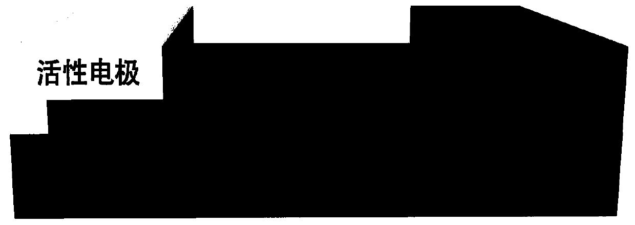
[0056] 3) Preparation of active electrode: use ultraviolet lithography or electron beam lithography to design an active electrode pattern at the other end of the two-dimensional atomic crystal at a distance of 300 nm from the inert electrode, then use electron beam evaporation to evaporate a 50 nm thick silver electrode, and finally peel it off to obtain active silver electrode.
Embodiment 2
[0058] 1) Preparation and transfer of germanium sulfide: peel off the germanium sulfide film to SiO by mechanical stripping 2 / Si substrate surface, the thickness of the film is about 20nm, and then in Ar / H 2 (Flow rate 100 / 5sccm), annealing at 300°C for one hour;
[0059] 2) Preparation of inert electrode: Design an inert electrode pattern on one end of the two-dimensional atomic crystal by ultraviolet lithography or electron beam lithography, then use electron beam evaporation to evaporate a 50nm thick gold electrode, and finally peel off to obtain an inert gold electrode;
[0060] 3) Preparation of active electrode: use ultraviolet lithography or electron beam lithography to design an active electrode pattern at the other end of the two-dimensional atomic crystal at a distance of 300 nm from the inert electrode, then use electron beam evaporation to evaporate a 50 nm thick silver electrode, and finally peel it off to obtain active silver electrode.
Embodiment 3
[0062] 1) Preparation and transfer of tin sulfide: peel off the tin sulfide film to SiO by mechanical stripping 2 / Si substrate surface, the thickness of the film is about 20nm, and then in Ar / H 2 (Flow rate 100 / 5sccm), annealing at 300°C for one hour;
[0063] 2) Preparation of inert electrode: Design an inert electrode pattern on one end of the two-dimensional atomic crystal by ultraviolet lithography or electron beam lithography, then use electron beam evaporation to evaporate a 50nm thick gold electrode, and finally peel off to obtain an inert gold electrode;
[0064] 3) Preparation of active electrode: use ultraviolet lithography or electron beam lithography to design an active electrode pattern at the other end of the two-dimensional atomic crystal at a distance of 300 nm from the inert electrode, then use electron beam evaporation to evaporate a 50 nm thick silver electrode, and finally peel it off to obtain active silver electrode.
PUM
| Property | Measurement | Unit |
|---|---|---|
| distance | aaaaa | aaaaa |
| distance | aaaaa | aaaaa |
| thickness | aaaaa | aaaaa |
Abstract
Description
Claims
Application Information
 - R&D
- Intellectual Property
- Life Sciences
- Materials
- Tech Scout
- Unparalleled Data Quality
- Higher Quality Content
- 60% Fewer Hallucinations
Browse by: Latest US Patents, China's latest patents, Technical Efficacy Thesaurus, Application Domain, Technology Topic, Popular Technical Reports.
© 2025 PatSnap. All rights reserved.Legal|Privacy policy|Modern Slavery Act Transparency Statement|Sitemap|About US| Contact US: help@patsnap.com