Etching method and etching gas for inner-side wall, and preparation method for nanowire device

A technology for etching gas and nanowires, applied in semiconductor/solid-state device manufacturing, electrical components, chemical instruments and methods, etc., can solve the problem that the high selection ratio of materials such as side wall silicon and top hard mask cannot be combined

Active Publication Date: 2020-03-31
INST OF MICROELECTRONICS CHINESE ACAD OF SCI
View PDF4 Cites 2 Cited by
  • Summary
  • Abstract
  • Description
  • Claims
  • Application Information

AI Technical Summary

Problems solved by technology

[0006] In view of the above analysis, the present invention aims to provide an etching method for the inner wall, an etching gas and a method for preparing a nanowire device, so as to solve the problem that the existing etching method retains the side wall material and the silicon and the top in the groove. The problem that the high selection ratio of materials such as hard masks cannot be achieved at the same time

Method used


Image

  • Etching method and etching gas for inner-side wall, and preparation method for nanowire device
  • Etching method and etching gas for inner-side wall, and preparation method for nanowire device
  • Etching method and etching gas for inner-side wall, and preparation method for nanowire device

Examples


Embodiment 1

[0052] A specific embodiment of the present invention discloses a gas for etching the inner wall of a nanowire device, the composition of the etching gas is: CH 2 f 2 、CH 4 , O 2 and Ar.

[0053] Compared with the prior art, by optimizing the composition of the etching gas in this embodiment, not only can the sidewall material in the groove be retained, but also a high selectivity ratio for materials such as silicon and the top hard mask can be achieved, and the selectivity ratio is not low. At 5:1.

[0054] Specifically, each component CH in the above etching gas 2 f 2 / CH 4 / O 2 The ratio of / Ar is 1:1:1:2˜1:1:1:5, and by controlling the ratio, the etching morphology can be precisely controlled.

Embodiment 2

[0056] Another specific embodiment of the present invention discloses a method for etching the inner wall of a nanowire device. In this etching method, the etching gas of Example 1 is used, and the flow rate of each component in the etching process is CH 2 f 2 : 10~30sccm, CH 4 : 10~30sccm, O 2 : 10-30 sccm, Ar40-100 sccm.

[0057] Compared with the prior art, the etching method provided in this embodiment controls the flow rate of each component in the etching gas to CH 2 f 2 : 10~30sccm, CH 4 : 10~30sccm, O 2 : 10~30sccm, Ar 40~100sccm, which can not only ensure a certain etching rate (not less than 1nm / min), but also ensure the corrosion of other materials such as SiO 2 The high selectivity ratio of etching, the selectivity ratio is not lower than 5:1, and there will be no sidewall roughness.

[0058] Specifically, when CH 2 f 2 When the flow rate is lower than 10 sccm, the etching stops; when the flow rate is higher than 30 sccm, the etching selection for other m...

Embodiment 3

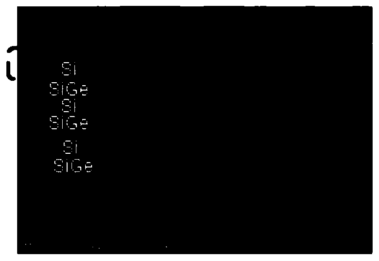
[0071] Yet another specific embodiment of the present invention, such as Figure 5 and Figure 6 As shown, a preparation method of a nanowire device is disclosed, comprising the following steps:

[0072] Step S1: Epitaxial Si and SiGe stack and SiO on the substrate 2 and / or SiN hard mask;

[0073] Step S2: Using an oxidation process, the two ends of the SiGe layer generate germanium oxide, and the two ends of the Si layer generate silicon oxide, using CF 4 / C 4 f 8 Plasma selective etching, removing the germanium oxide generated by oxidation in the SiGe layer, so that a filling gap of a predetermined length is formed between the remaining SiGe layer and the adjacent Si layer with silicon oxide at both ends;

[0074] Step S3: depositing inner wall material in the filled void and on the exposed surface of other structural layers;

[0075] Step S4: Using the etching method of Embodiment 2 to remove the material of the inner wall except for filling the gap, to form the inner...


PUM


Abstract

The invention relates to an etching method and etching gas for an inner-side wall, and a preparation method for a nanowire device, belonging to the technical field of semiconductors. The invention solves the problem of incapability of simultaneously realizing reservation of a side-wall material in a groove and high selection ratio of materials like silicon and a top-part hard mask in the prior art. The gas used for etching the inner-side wall of the nanowire device comprises CH2F2, CH4, O2 and Ar, wherein the ratio of the CH2F2 to the CH4 to the O2 to the Ar is 1: 1: 1: 2 to 1: 1: 1: 5; in theetching process, an upper radio frequency power is in a range of 100-1000 W, and a lower radio frequency power is in a range of 10-80 W; the power of a lower electrode is 0-60 W; and the temperatureof a base is minus 20 DEG C to 90 DEG C. The preparation method for the nanowire device comprises the following steps: extending a lamination layer and a hard mask on a substrate; transversely etchingan SiGe layer so as to form a filling gap with a preset length; depositing an inner-side wall material; and carrying out etching to remove the inner-side wall material outside the filling gap so as to form the inner-side wall. According to the invention, the side-wall material in the groove can be reserved, and high selection ratio of materials like the silicon and the top-part hard mask can be achieved.

Description

technical field [0001] The invention relates to the technical field of semiconductors, in particular to an etching method of an inner wall, an etching gas and a preparation method of a nanowire device. Background technique [0002] After CMOS enters the 3-5nm technology generation, in order to enhance device gate control and overcome short channel effects, stacked gate-all-around devices (GAA) will be the mainstream development direction, and the inner wall is a very important technology (as shown in the flow chart). It can control the effective gate length and reduce the leakage between the gate and the source and drain and reduce the effect of parasitic capacitance. However, the formation of the inner wall requires precise anisotropy. It has a high selection ratio for materials other than the inner wall, and can strictly control the etching precision. It is necessary to ensure that there is no sidewall material residue at the end of the nanowire, and it must also be concav...

Claims


Application Information

Patent Timeline
IPC IPC(8): C09K13/00H01L21/311
CPCC09K13/00H01L21/31116H01L21/31144
Inventor 李俊杰周娜李永亮王桂磊张青竹杨涛殷华湘李俊峰王文武
Owner INST OF MICROELECTRONICS CHINESE ACAD OF SCI
Why Eureka
Try Eureka