
VCSEL chip and preparation method thereof

A chip and confinement layer technology, applied in the field of VCSEL, can solve the problems of high photon confinement and carrier confinement at the same time, small carrier gain, complex process, etc., to improve fundamental mode capability and reduce edge mode The effect of producing and reducing the absorption of impurities

Pending Publication Date: 2020-03-31
XIAMEN QIANZHAO SEMICON TECH CO LTD
View PDF1 Cites 0 Cited by
  • Summary
  • Abstract
  • Description
  • Claims
  • Application Information

AI Technical Summary

Problems solved by technology

[0006] The purpose of the present invention is to provide a VCSEL chip and its preparation method to solve the problem of low carrier gain in the active region, inability to simultaneously have high photon confinement and carrier confinement, complex process and high cost in the prior art. high problem

Method used


Image

  • VCSEL chip and preparation method thereof
  • VCSEL chip and preparation method thereof

Examples


Embodiment 1

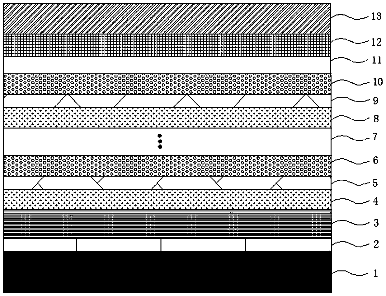
[0055] Such as figure 1 Shown, a kind of preparation method of VCSEL chip comprises:

[0056] Provide a substrate 1;

[0057] On the surface of the substrate 1, a buffer layer 2, an N-type DBR layer 3, an N-type confinement layer 4, a first waveguide layer 5, a second waveguide layer 6, a quantum well 7, a second symmetric waveguide layer 8, and a first symmetric waveguide are sequentially grown. Layer 9, P-type confinement layer 10; N-type confinement layer 4, first waveguide layer 5, second waveguide layer 6, second symmetric waveguide layer 8, first symmetric waveguide layer 9, P-type confinement layer 10 all include Al x GaAs layer, where X is the elemental composition of Al, and the first waveguide layer 5 and the first symmetrical waveguide layer 9 are respectively obtained through the modulation process of gradually changing the function of the potential barrier, specifically: by passing the flow rate to the Al element respectively , Ga element flow rate and Al elemen...

Embodiment 2

[0091] Such as figure 1 Shown, a kind of preparation method of VCSEL chip comprises:

[0092] Provide a substrate 1;

[0093] On the surface of the substrate 1, a buffer layer 2, an N-type DBR layer 3, an N-type confinement layer 4, a first waveguide layer 5, a second waveguide layer 6, a quantum well 7, a second symmetric waveguide layer 8, and a first symmetric waveguide are sequentially grown. Layer 9, P-type confinement layer 10; N-type confinement layer 4, first waveguide layer 5, second waveguide layer 6, second symmetric waveguide layer 8, first symmetric waveguide layer 9, P-type confinement layer 10 all include Al x Ga y In z In the P layer, X is the elemental composition of Al, and the first waveguide layer 5 and the first symmetrical waveguide layer 9 are respectively obtained through the modulation process of gradually changing the function of the potential barrier, specifically: by passing the flow rate to the Al element respectively , Ga element flow rate and...

Embodiment 3

[0127] Such as figure 1 Shown, a kind of preparation method of VCSEL chip comprises:

[0128] Provide a substrate 1;

[0129] On the surface of the substrate 1, a buffer layer 2, an N-type DBR layer 3, an N-type confinement layer 4, a first waveguide layer 5, a second waveguide layer 6, a quantum well 7, a second symmetric waveguide layer 8, and a first symmetric waveguide are sequentially grown. Layer 9, P-type confinement layer 10; N-type confinement layer 4, first waveguide layer 5, second waveguide layer 6, second symmetric waveguide layer 8, first symmetric waveguide layer 9, P-type confinement layer 10 all include Al x In y GaAs layer, where X is the elemental composition of Al, and the first waveguide layer 5 and the first symmetrical waveguide layer 9 are respectively obtained through the modulation process of gradually changing the function of the potential barrier, specifically: by passing the flow rate to the Al element respectively , Ga element flow rate and Al ...


PUM

PropertyMeasurementUnit
Thicknessaaaaaaaaaa
Thicknessaaaaaaaaaa
Thicknessaaaaaaaaaa

Abstract

According to the VCSEL chip and the preparation method thereof provided by the invention, the first symmetrical waveguide layer is arranged between the second symmetrical waveguide layer and the P-type limiting layer, so that the barrier difference caused by different Al components of the second symmetrical waveguide layer and the P-type limiting layer can be effectively reduced; secondly, the potential barrier of the first symmetrical waveguide layer is in function gradual change, so that the potential barriers of the head end point and the tail end point of the first symmetrical waveguide layer are infinitely close to the potential barriers of the second symmetrical waveguide layer and the P-type limiting layer respectively, the potential barrier junction of the second symmetrical waveguide layer and the P-type limiting layer is reduced to a greater extent, and a better series resistance value is obtained; and thirdly, through the transition of the first symmetrical waveguide layer,low resistance is formed between the second symmetrical waveguide layer and the P-type limiting layer, so that the heat loss of the VCSEL chip is reduced to a certain extent, and the effect of improving the differential gain of the VCSEL chip is further achieved.

Description

technical field [0001] The invention relates to the technical field of VCSEL, in particular to a VCSEL chip and a preparation method thereof. Background technique [0002] VCSEL, the full name is Vertical Cavity Surface Emitting Laser (Vertical Cavity Surface Emitting Laser), developed on the basis of gallium arsenide semiconductor materials, different from other light sources such as LED (light emitting diode) and LD (Laser Diode, laser diode), has a volume Small, circular output spot, single longitudinal mode output, low threshold current, low price, easy integration into large-area arrays, etc., are widely used in optical communication, optical interconnection, optical storage and other fields. [0003] The epitaxial structure of the existing VCSEL laser usually includes a substrate on which a buffer layer, an N-type doped DBR, an active layer, an oxidation confinement layer, a P-type doped DBR, and a P-type cladding layer are sequentially deposited. ; Wherein, the activ...

Claims


Application Information

Patent Timeline
IPC IPC(8): H01S5/183H01S5/20
CPCH01S5/183H01S5/2018H01S5/2031
Inventor 田宇
Owner XIAMEN QIANZHAO SEMICON TECH CO LTD
Learn More