Large-area high-quality graphene lossless transfer method based on doping layer assistance
A transfer method, single-layer graphene technology, applied in the direction of single-layer graphene, graphene, chemical instruments and methods, etc., can solve problems such as poor electrical performance, graphene material contamination, film damage, etc., to achieve low cost, Simple operation, powerful function effect
- Summary
- Abstract
- Description
- Claims
- Application Information
AI Technical Summary
Problems solved by technology
Method used
Image
Examples
preparation example Construction
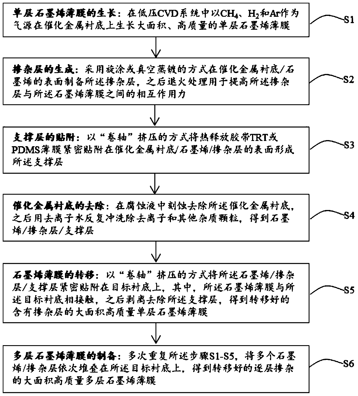
[0051] The present invention also provides a method for preparing a large-area high-quality multilayer graphene film, such as image 3 , 4 As shown, on the basis of the preparation of the above-mentioned large-area high-quality single-layer graphene film containing a doped layer, the following steps are also included:
[0052] S6, preparation of large-area high-quality multilayer graphene film: repeat the steps S1-S5 multiple times, stack multiple graphene / doped layers on the target substrate 5 in sequence, and obtain a transferred layer by layer Doped large-area high-quality multilayer graphene films.
[0053] Among them, the number of layers of the large-area high-quality multilayer graphene film doped layer by layer can be designed, and can be flexibly adjusted according to actual needs; the thickness and type of each doped layer can be independently designed, which can realize multilayer graphene Gradient doping of thin films or sudden doping of P-type / N-type alternately...
Embodiment 1
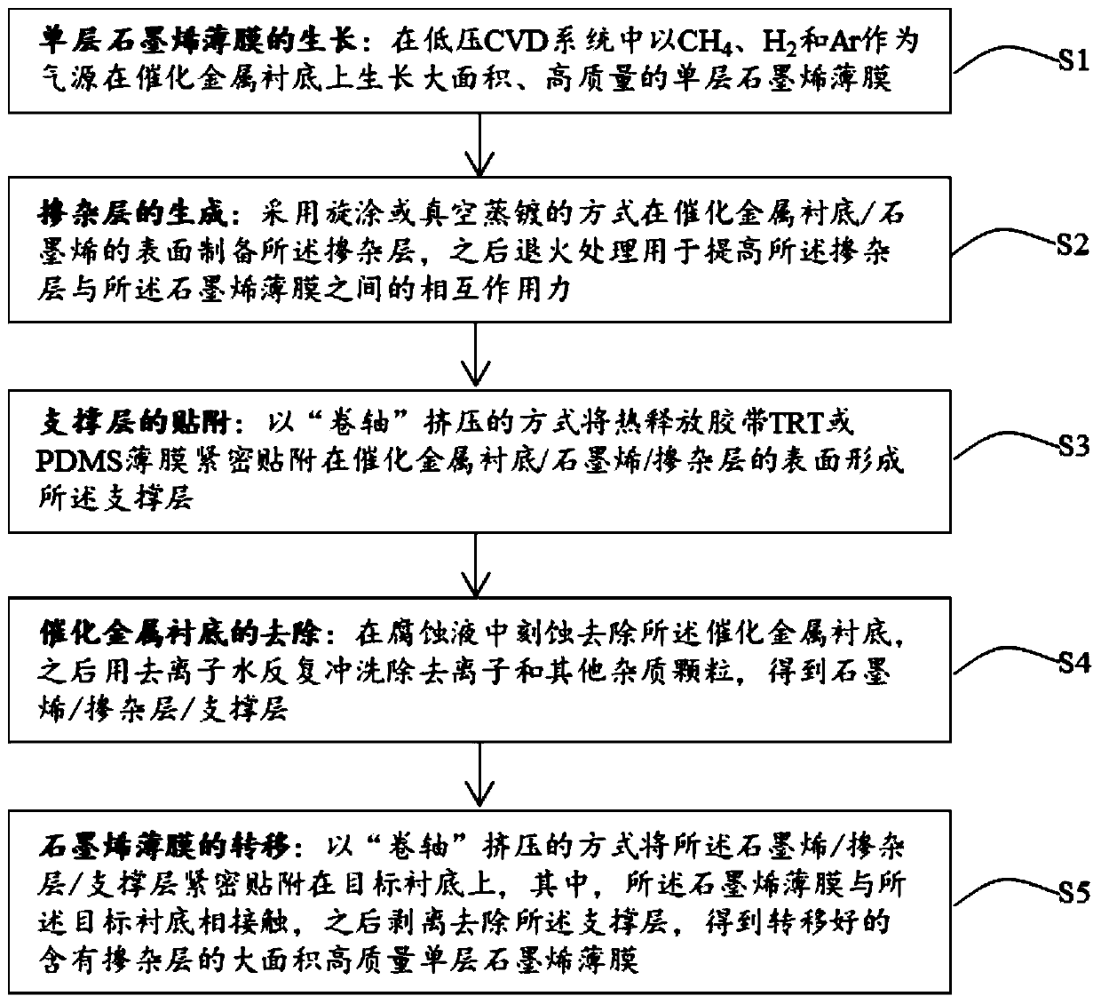
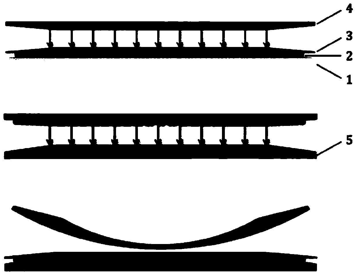
[0060] Process parameter selection: the catalytic metal substrate 1 is polycrystalline Cu foil; the doped layer 3 is made of perfluorosulfonic acid PFSA, which is prepared by solution spin coating with a concentration of 5 mg / ml; the support layer 4 is thermal release tape TRT; the target The substrate 5 is glass. A large-area high-quality single-layer graphene film non-destructive transfer method containing a perfluorosulfonic acid PFSA doped layer, comprising the following steps:
[0061] S1. A low-pressure CVD system is used to grow a single-layer graphene 2 film on Cu. The 25um thick polycrystalline Cu foil 1 is cleaned in 10% hydrochloric acid to remove the oxide layer; the CVD chamber is evacuated to 50mTorr, and the 2 and 10sccmAr atmosphere to 1000°C; high temperature annealing of polycrystalline Cu foil for 1 30min to improve its crystal quality; stepwise introduction of CH 4 (3sccm-20min&6sccm-60min) grow graphene film 2, control the nucleation point density of grap...
PUM
 Abstract
Description
Claims
Application Information


