GaN-based lateral super junction device and manufacturing method thereof
A technology of superjunction device and fabrication method, which is applied in semiconductor/solid-state device manufacturing, semiconductor devices, electrical components, etc., can solve the problems that GaAs power devices cannot meet technological development, narrow band gap, and low breakdown electric field, etc. Small on-resistance, high breakdown voltage and good repeatability
- Summary
- Abstract
- Description
- Claims
- Application Information
AI Technical Summary
Problems solved by technology
Method used
Image

Examples
Embodiment 1
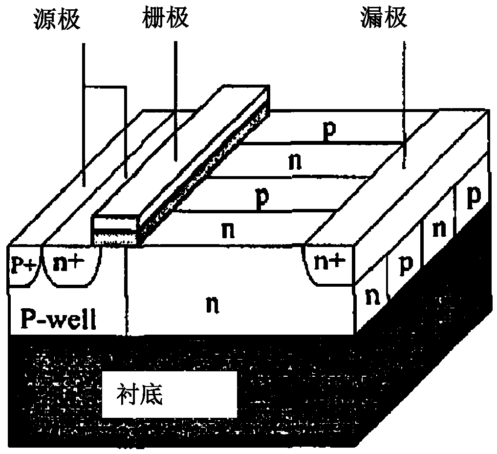
[0131] see Figure 2a , Figure 2b , a GaN-based lateral superjunction device, which includes a substrate 1, a buffer layer 2 disposed on the substrate 1, a heterojunction disposed on the buffer layer 2, the heterojunction includes a first semiconductor 3 and a second semiconductor 4. The second semiconductor 4 is formed on the first semiconductor 3, and a two-dimensional electron gas is formed between the first semiconductor and the second semiconductor; a source 7, a drain 8, and a gate 9 are arranged on the heterojunction, The source electrode 7 and the drain electrode 8 are all arranged on the second semiconductor 4, and the source electrode and the drain electrode are electrically connected through the two-dimensional electron gas, and the second semiconductor 4 is also provided with a plurality of P-type semiconductors 5 oriented The P-type semiconductor array formed by arrangement, the two ends of the P-type semiconductor 5 point to the source 7 and the drain 8 respect...
Embodiment 2
[0133] A fabrication process of a GaN-based lateral superjunction device may include the following steps:
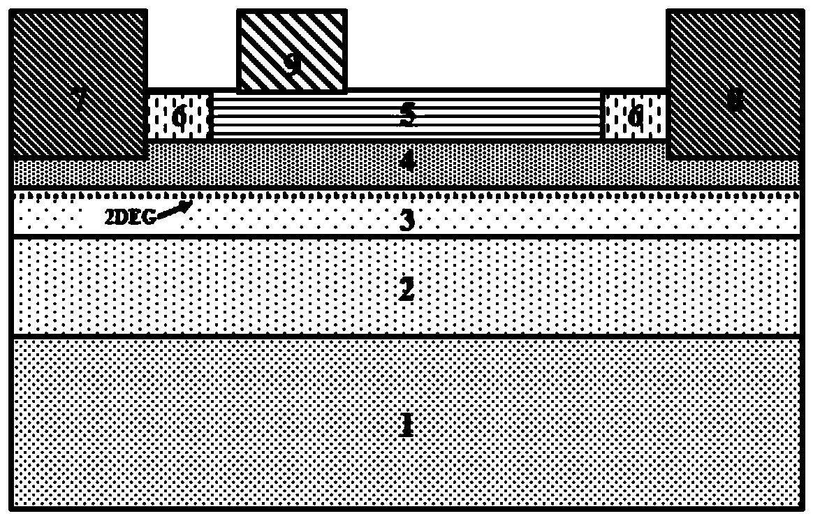
[0134] 1) using metal organic chemical vapor deposition (MOCVD) method to grow such as image 3 In the material structure shown, the substrate is made of Si with a thickness of 400 μm, and the buffer layer is made of high-resistance GaN with a thickness of 4.2 μm; in the AlGaN / GaN heterostructure, the thickness of GaN is 260 nm, the thickness of AlGaN is 18 nm, and the Al component content is 18 nm. %; The P-type semiconductor is made of P-GaN material, and the thickness of P-GaN is 70nm;
[0135] 2) Use inductively coupled plasma to etch the P-GaN layer in the ohmic region, and then use electron beam evaporation technology to deposit Ti / Al / Ni / Au four-layer metal and layer it on N 2 Annealed at 875°C for 30s under the same conditions, the structure of the formed material is as follows Figure 4 shown;
[0136] 3) Use hydrogen plasma to treat part of P-GaN to form high...
Embodiment 3
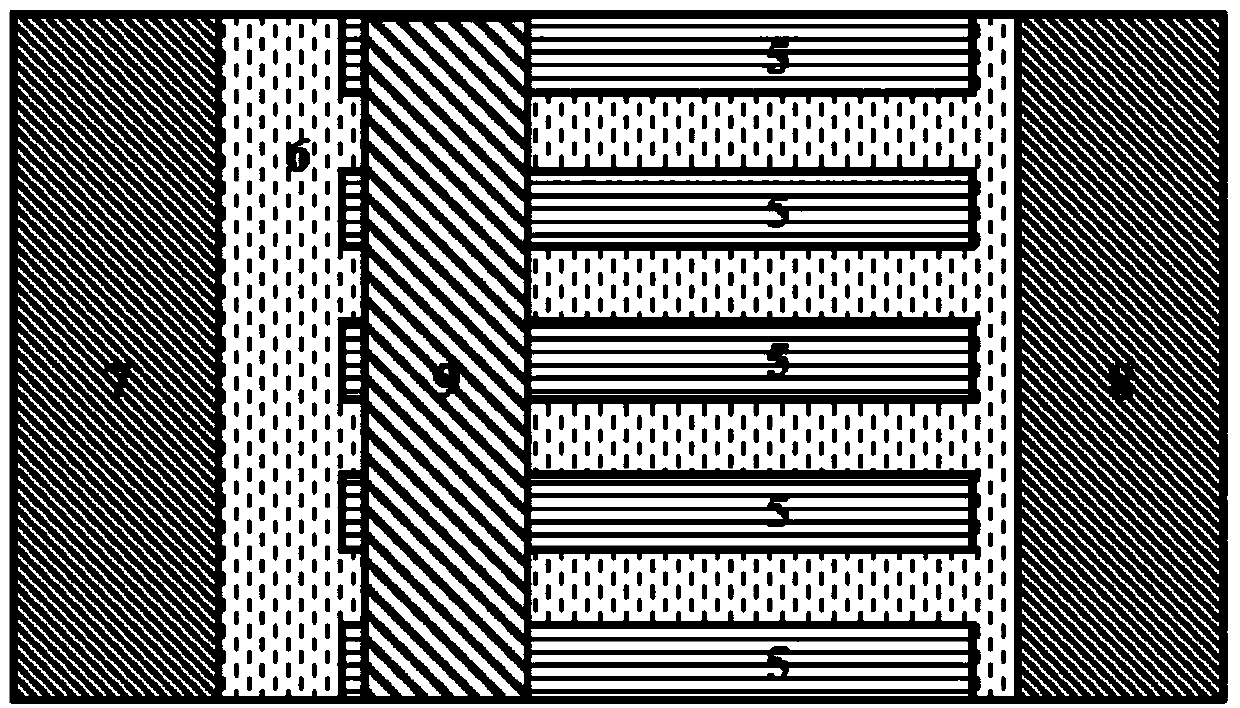
[0139] see Figure 7a , Figure 7b , a GaN-based lateral superjunction device, which includes a substrate 1, a buffer layer 2 disposed on the substrate 1, a heterojunction disposed on the buffer layer 2, the heterojunction includes a first semiconductor 3 and a second semiconductor 4. The second semiconductor 4 is formed on the first semiconductor 3, and a two-dimensional electron gas is formed between the first semiconductor and the second semiconductor; a source 7, a drain 8, and a gate 9 are arranged on the heterojunction, The source and the drain are electrically connected through the two-dimensional electron gas, and a P-type semiconductor array formed by a plurality of P-type semiconductors 5 is arranged on the first semiconductor 3. The two P-type semiconductor arrays The terminals point to the source 7 and the drain 8 respectively, the source 7 and the drain 8 are connected to the second semiconductor 4, the gate 9 is located between the source 7 and the drain 8, and ...
PUM
| Property | Measurement | Unit |
|---|---|---|
| Thickness | aaaaa | aaaaa |
| Thickness | aaaaa | aaaaa |
| Thickness | aaaaa | aaaaa |
Abstract
Description
Claims
Application Information
PatSnap Eureka turns technology decisions into work you can execute. Powered by our Innovation Knowledge Graph, it runs expert workflows across engineering, life sciences, materials and intellectual property. Get your review-ready output in minutes.


