On-chip multi-band terahertz three-dimensional antenna

A three-dimensional antenna, terahertz technology, applied in the direction of antenna grounding switch structure connection, radiation element structure, etc., can solve the problems of low gain, narrow bandwidth, single frequency band, etc., and achieve bandwidth and gain improvement, size reduction, and increase area Effect

Active Publication Date: 2020-04-24
TERAPARK TECH (NANJING) CO LTD
View PDF8 Cites 3 Cited by
  • Summary
  • Abstract
  • Description
  • Claims
  • Application Information

AI Technical Summary

Problems solved by technology

But there are also disadvantages of single frequency band, narrow bandwidth and low gain.

Method used


Image

  • On-chip multi-band terahertz three-dimensional antenna
  • On-chip multi-band terahertz three-dimensional antenna
  • On-chip multi-band terahertz three-dimensional antenna

Examples


Embodiment Construction

[0020] The present invention is an on-chip multi-band terahertz stereo antenna design, which will be clearly and completely described below in conjunction with the technical solutions in the embodiments of the invention.

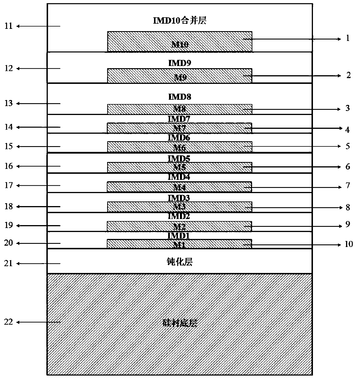
[0021] Such as figure 1 As shown, it is a schematic sectional view of the process of the present invention. There are 12 dielectric layers from top to bottom, and from top to bottom are IMD10 combined layer, IMD9 dielectric layer, IMD8 dielectric layer, IMD7 dielectric layer, IMD6 dielectric layer, and IMD5 Dielectric layer, IMD4 dielectric layer, IMD3 dielectric layer, IMD2 dielectric layer, IMD1 dielectric layer, passivation layer and silicon substrate layer. 11 to 22 in sequence, 11 is the IMD10 combined layer with a thickness of 5.275 μm and a relative dielectric constant of 4.65; 12 is the IMD9 dielectric layer with a thickness of 1.59 μm and a relative dielectric constant of 4.48; 13 is the IMD8 dielectric layer with a thickness of 0.74μm, the relativ...


PUM

PropertyMeasurementUnit
thicknessaaaaaaaaaa
thicknessaaaaaaaaaa
thicknessaaaaaaaaaa

Abstract

The invention discloses an on-chip multi-band terahertz three-dimensional antenna. The antenna is mainly composed of ten radiation patches and ten NMOS transistor switches. The characteristics of multi-layer metal of a TSMC 40nm CMOS process are utilized. A planar antenna structure is changed into a three-dimensional structure. Each layer of metal of M1 to M10 is designed into a rectangular radiation patch with a simple structure. An I-shaped groove is formed in the middle. A section of microstrip transmission line is led out to be connected with a source electrode of an NMOS tube. A microstrip feeder line is connected with a drain electrode of the NMOS tube, and a grid electrode of the NMOS tube is connected with bias voltage. By adjusting the grid bias voltage of the NMOS tube and conducting the NMOS tube, a switch is closed, and a layer of radiation patch is added to the antenna, so that the shape of the antenna is changed, and a new working frequency is obtained. When all the switches are closed, the antenna is of a three-dimensional structure formed by connecting ten layers of radiation patches, and various different working frequencies can be achieved. Besides, the antenna and a terahertz circuit are integrated on the same chip, and a terahertz detector is designed, so that a multi-band detection function can be realized.

Description

technical field [0001] The invention belongs to the field of antenna structure design. In particular, it is an on-chip multi-band terahertz stereo antenna. Background technique [0002] Terahertz (THz) generally refers to electromagnetic waves with a frequency range of 100 GHz to 10 THz and a wavelength range of 30 μm to 3 mm, which is between millimeter waves and infrared light in the electromagnetic spectrum. As the last frequency window to be fully studied in the electromagnetic spectrum, the terahertz frequency band has not been fully recognized and applied, so it is called "terahertz gap (THz Gap)". Compared with electromagnetic waves of other frequencies in the electromagnetic spectrum, terahertz waves have many unique response characteristics, such as transient, non-destructive, high penetration, low energy, etc., making their advantages as a detection technology gradually prominent, and can realize True non-destructive detection. Compared with detectors in the for...

Claims


Application Information

Patent Timeline
Patent Type & Authority Applications(China)
IPC IPC(8): H01Q1/36H01Q1/38H01Q1/50
CPCH01Q1/36H01Q1/38H01Q1/50
Inventor 徐雷钧殷鹏程白雪
Owner TERAPARK TECH (NANJING) CO LTD
Why Eureka
Try Eureka