Eureka AIR delivers breakthrough ideas for toughest innovation challenges, trusted by R&D personnel around the world.

Method for realizing IGZO photocurrent regulation and control based on two-dimensional black phosphorus material

A black phosphorus and construction method technology, applied in the direction of circuits, electrical components, sustainable manufacturing/processing, etc., can solve the problems of complex preparation process of heterojunction devices, small sample size, unstable device performance, etc., and achieve photocurrent intensity and response time Effective, repeatable, easy-to-achieve effects

Active Publication Date: 2020-04-28
JIANGNAN UNIV
View PDF4 Cites 1 Cited by
  • Summary
  • Abstract
  • Description
  • Claims
  • Application Information

AI Technical Summary

Problems solved by technology

However, the above-mentioned heterostructures are all based on two-dimensional materials, the sample size is small, the transfer of the heterojunction and the preparation process of the device are relatively complicated, and the device performance is not stable enough.

Method used


Image

  • Method for realizing IGZO photocurrent regulation and control based on two-dimensional black phosphorus material
  • Method for realizing IGZO photocurrent regulation and control based on two-dimensional black phosphorus material
  • Method for realizing IGZO photocurrent regulation and control based on two-dimensional black phosphorus material

Examples


Embodiment 1

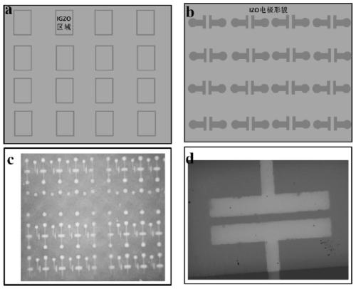
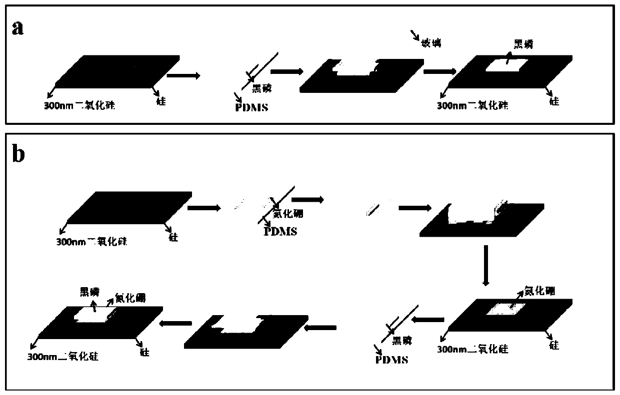
[0060] based on figure 1 Using the mask to prepare IGZO devices, the preparation process includes the following steps:

[0061] (1) Preparing the mask: draw the mask according to the needs of the experiment (such as figure 1 (a) and (b)). In this example, a set of masks are used, one of which is used to prepare the IGZO channel layer (mask I), and the other is used to prepare electrodes on the surface of IGZO (Mask plate II). The channel width of mask plate I is 40um. Find a mask manufacturer for processing (the manufacturer found in this example is a micro-nano scientific research laboratory equipment company), in order to ensure the mask Flatness and thinner thickness, the original material used is a stainless steel plate with a thickness of 3mm;

[0062] (2) Substrate cleaning: In this embodiment, a silicon wafer plated with a 300nm silicon dioxide layer is used as the substrate, and the substrates are placed in acetone, ethanol, and deionized water for 5 minutes in order to rem...

Embodiment 2

[0079] Example 2 Changing the IGZO channel width

[0080] Use mask to prepare IGZO device:

[0081] (1) Preparing the mask: The difference from the mask in Example 1 is that the channel width of the mask I in this embodiment is 80 um; the materials and processing manufacturers are the same;

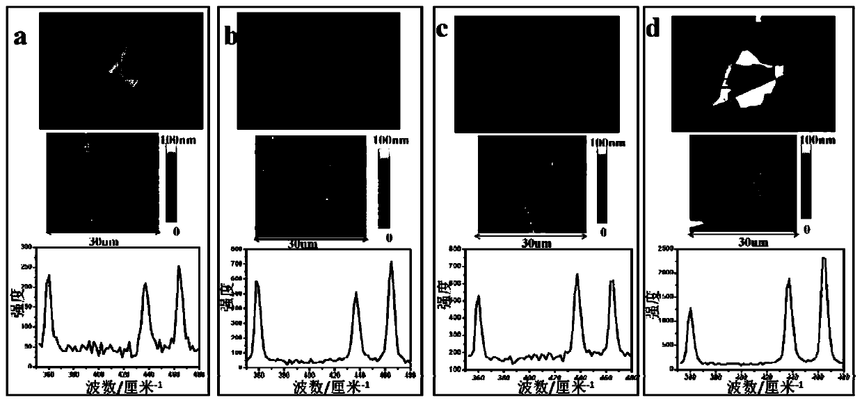
[0082] (2)~(5): Same as (2)~(5) in Example 1, fabricated an IGZO device with a channel width of 80um; fabricated black phosphorus-IGZO heterogeneous structures with different structures: the same as in Example 1. The preparation method is the same, and four types of black phosphorus-IGZO heterogenes are prepared.

[0083] Characterization of the photocurrent performance of different types of heterojunctions (type I and type III): the photocurrent was tested using the test method in Example 1.

[0084] The test result is like Image 6 : In Type I, that is, after black phosphorus covers the electrodes at both ends of the channel, the photocurrent in the original IGZO decreases, but the decrease is n...

Embodiment 3

[0085] Example 3 Changing the thickness of IGZO channel

[0086] (1)~(2): Same as (1)~(2) in Example 1;

[0087] (3) Use a clamp to fix the stainless steel mask on the surface of the substrate that has been cut in advance and the same size as the mask. By controlling the clamp, the mask and the substrate are in close contact with each other, so as to avoid any channel in the magnetron sputtering process. Infiltrated IGZO; use magnetron sputtering method to deposit IGZO, put the substrate with fixed mask into the magnetron sputtering chamber, evacuate to below 10Pa, and then pass in argon and oxygen, the flow rates of which are respectively 10mL / min and 0.3mL / min, reaction pressure is 400mPa, sputtering power is 1.76W / cm 2 , Sputtering time is 12min; prepare 40nm IGZO channel;

[0088] (4) to (5): the same as in Example 1.

[0089] Preparation of black phosphorus-IGZO heterojunctions with different structures: the same as the preparation method in Example 1, the black phosphorus-IGZO ...


PUM

PropertyMeasurementUnit
thicknessaaaaaaaaaa
thicknessaaaaaaaaaa
band gapaaaaaaaaaa

Abstract

The invention discloses a method for realizing IGZO photocurrent regulation and control based on a two-dimensional black phosphorus material, and belongs to the field of semiconductor devices. The invention provides a method for preparing an IGZO-black phosphorus heterostructure by using a dry transfer technology. The contact mode between IGZO and black phosphorus is changed; regulation and control of IGZO on photocurrent response of different laser wavelengths can be realized; according to the method, an IGZO channel and the electrode are subjected to magnetron sputtering by virtue of a maskplate, the repeatability is good, large-area multi-device preparation can be realized, a black phosphorus sample is prepared by virtue of a mechanical stripping method, the thickness and the size arecontrollable, a heterojunction is prepared by virtue of a dry transfer technology, operation is simple, and the controllability is high. The method is beneficial to promoting the development of the IGZO film in the micro-nano field and the semiconductor industry.

Description

Technical field [0001] The invention relates to a method for realizing IGZO photocurrent control based on a two-dimensional black phosphorous material, and belongs to the field of semiconductor devices. Background technique [0002] Amorphous indium gallium zinc oxide (IGZO for short) is a new type of transparent oxide semiconductor material with a wide band gap (~3.5eV) and high mobility (~35.8cm) 2 V -1 s -1 ), low preparation temperature and extremely high stability, which are the current research hotspots in the field of display technology, and are also considered to be an important material in the development of flexible display technology, flexible wearable electronic technology and new sensor technology . In 2004, researchers such as Hosono and Nomura used IGZO for the first time to fabricate a fully transparent PET thin film transistor (TFT) on a flexible substrate at room temperature, with a field-effect mobility exceeding 10cm. 2 V - 1 s -1 , Which is an order of magnit...

Claims


Application Information

Patent Timeline
Patent Type & Authority Applications(China)
IPC IPC(8): H01L31/18H01L31/0336
CPCH01L31/18H01L31/0336Y02P70/50H01L31/109H01L31/032H01L31/1884
Inventor 南海燕李大庆邵枫肖少庆顾晓峰
Owner JIANGNAN UNIV
Why Eureka
Eureka Blog
Learn More