Single-layer tin disulfide thin film and two-dimensional heterojunction and preparation method thereof

A two-dimensional heterojunction and tin disulfide technology, which is applied in electrical components, circuits, semiconductor devices, etc., can solve the problems of immature tin disulfide film preparation process and difficulty in obtaining single-layer films.

Inactive Publication Date: 2020-05-05
XIAMEN UNIV
View PDF3 Cites 5 Cited by
  • Summary
  • Abstract
  • Description
  • Claims
  • Application Information

AI Technical Summary

Problems solved by technology

At present, the preparation process of tin disulfide thin film is not yet mature, and most of them form nanostructures of different shapes, and it is not easy to obtain a single-layer thin film

Method used


Image

  • Single-layer tin disulfide thin film and two-dimensional heterojunction and preparation method thereof
  • Single-layer tin disulfide thin film and two-dimensional heterojunction and preparation method thereof
  • Single-layer tin disulfide thin film and two-dimensional heterojunction and preparation method thereof

Examples


Embodiment 1

[0035] This embodiment provides a single-layer tin disulfide thin film and its two-dimensional heterojunction and preparation method.

[0036] 1.1 The preparation method comprises the following steps:

[0037] a) Preparation of epitaxial substrate:

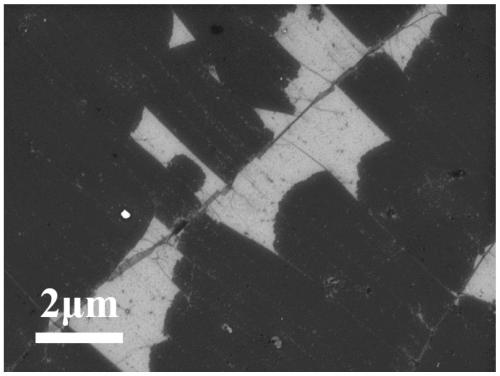
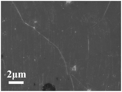
[0038]Using chemical vapor deposition method, catalytic cracking of methane on the metal surface at 1030°C with the assistance of hydrogen to generate a single layer of graphene covering the metal surface;

[0039] Subsequently, single-layer graphene was transferred to the supporting substrate SiO by spin-coating PMMA followed by dissolution of the metal substrate or bubbling method. 2 On / Si, the epitaxial substrate is prepared; among them, the selected SiO 2 / SiO in Si substrate 2 The thickness is 90nm.

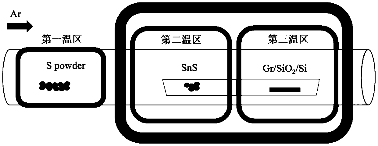
[0040] b) Preparation of the growth system:

[0041] Such as figure 1 , the quartz tube is divided into the first temperature zone, the second temperature zone and the third temperature zone. In this embodiment, a convent...


PUM

PropertyMeasurementUnit
thicknessaaaaaaaaaa
cover factoraaaaaaaaaa

Abstract

The invention discloses a single-layer tin disulfide thin film and a two-dimensional heterojunction and a preparation method thereof. Stannous sulfide powder and sulfur powder are used as raw materials, a large-area single-layer tin disulfide semiconductor thin film is prepared and generated on a graphene substrate by using a chemical vapor deposition method, and a novel two-dimensional vertical heterostructure is constructed. The single-layer tin disulfide film prepared by the method is flat in structure and uniform in thickness, and the size can be effectively controlled by changing processconditions; the two-dimensional heterojunction is formed by the single-layer tin disulfide thin film and a graphene film with the single atomic layer thickness, so that the structural characteristicsof a material system can be improved, and the single-layer tin disulfide thin film can be applied to a micro-nano optoelectronic device.

Description

technical field [0001] The invention belongs to the field of semiconductors and their manufacture, and in particular relates to a single-layer tin disulfide thin film, a two-dimensional heterojunction and a preparation method thereof. Background technique [0002] Graphene-like two-dimensional materials, such as transition metal chalcogenides, IIIA-VA, IVA-VIA compounds, etc., have been widely studied due to their tunable bandgap and potential applications in catalysis, electronics, optoelectronics, etc. focus on. Two-dimensional heterostructure materials, by stacking and arranging different two-dimensional materials in a certain order in a manner similar to Lego bricks, use the weak interaction between layers to realize the regulation and improvement of the properties of two-dimensional materials. This kind of two-dimensional heterostructure system with new physical and chemical properties is a hot spot in international scientific research. However, it is quite difficult ...

Claims


Application Information

Patent Timeline
Patent Type & Authority Applications(China)
IPC IPC(8): H01L29/16H01L29/165H01L29/24
CPCH01L29/1606H01L29/165H01L29/24
Inventor 周颖慧林高翔占林杰卢捷郑韬黄俊杰张悦蔡伟伟
Owner XIAMEN UNIV
Why Eureka
Try Eureka