Solar cell for all-black crystalline silicon photovoltaic module and preparation method of solar cell
A solar cell and photovoltaic module technology, applied in photovoltaic power generation, circuits, electrical components, etc., can solve the film thickness and refractive index differences, tubular PERC solar cells cannot meet the requirements of the appearance of all black photovoltaic modules, and the appearance is uneven, etc. problem, to achieve the effect of reducing reflectivity, good passivation and reducing reflectivity, eliminating unevenness
- Summary
- Abstract
- Description
- Claims
- Application Information
AI Technical Summary
Problems solved by technology
Method used
Image
Examples
preparation example Construction
[0096] Correspondingly, the present invention discloses a method for preparing a solar cell for an all black crystal silicon photovoltaic module, including:
[0097] (1) Select p-type silicon wafers, and clean the silicon wafers;
[0098] Specifically, a low-reflectance textured surface is prepared on the surface of the silicon wafer by methods such as alkali texturing or ion etching, and the frontal reflectance after texturing is 8.5% to 11.0%;
[0099] (2) Carry out n-type layer diffusion to the silicon wafer after cleaning the texture;
[0100] Specifically, gas phase diffusion or ion implantation is used, and the resistance after diffusion is 100Ω / sq~150Ω / sq;
[0101] (3) Perform SE laser process on the front side of the silicon wafer to form front side selective doping;
[0102] Specifically, the front side laser is used to process the n-type diffusion layer to form front side selective doping, and the square resistance of the selective doping area is 70Ω / sq~100Ω / sq;
...
Embodiment 1
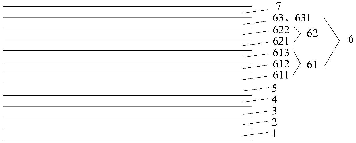
[0117] A solar cell for all-black crystal silicon photovoltaic modules, which sequentially includes a back silver electrode, a back aluminum film, a back composite film, a p-type silicon wafer, an n-type doped layer, a front composite film, and a front silver electrode from bottom to top,
[0118] Wherein, the front composite film includes a SiNx:Hy layer, a SiOxNy layer and a SiOx layer, the SiNx:Hy layer is connected to the n-type doped layer, and the SiOx layer is connected to the front silver electrode;
[0119] The SiNx:Hy layer is composed of 4 SiNx:Hy layers with different refractive indices and thicknesses, including the first SiNx:Hy layer, the second SiNx:Hy layer, the third SiNx:Hy layer and the fourth SiNx from bottom to top : Hy layer; the thickness of the first SiNx: Hy layer is 10nm, and the refractive index is 2.3; the thickness of the second SiNx: Hy layer is 12nm, and the refractive index is 2.16; the thickness of the third SiNx: Hy layer The thickness of the...
Embodiment 2
[0127] A solar cell for all-black crystal silicon photovoltaic modules, which sequentially includes a back silver electrode, a back aluminum film, a back composite film, a p-type silicon wafer, an n-type doped layer, a front composite film, and a front silver electrode from bottom to top,
[0128] Wherein, the front composite film includes a SiNx:Hy layer, a SiOxNy layer and a SiOx layer, the SiNx:Hy layer is connected to the n-type doped layer, and the SiOx layer is connected to the front silver electrode;
[0129] The SiNx:Hy layer is composed of 3 layers of SiNx:Hy layers with different refractive indices and thicknesses, including the first SiNx:Hy layer, the second SiNx:Hy layer, and the third SiNx:Hy layer from bottom to top; A SiNx:Hy layer has a thickness of 12nm and a refractive index of 2.25; the second SiNx:Hy layer has a thickness of 10nm and a refractive index of 2.15; the third SiNx:Hy layer has a thickness of 13nm and a refractive index of 2.10 .
[0130] The S...
PUM
| Property | Measurement | Unit |
|---|---|---|
| thickness | aaaaa | aaaaa |
| thickness | aaaaa | aaaaa |
| thickness | aaaaa | aaaaa |
Abstract
Description
Claims
Application Information

