Silicon carbide trench IGBT structure and manufacturing method thereof

A technology of silicon carbide grooves and grooves, which is applied in semiconductor/solid-state device manufacturing, high-efficiency power electronic conversion, electrical components, etc., can solve the problems of long current tailing of devices, increase of device turn-off loss, etc., and reduce on-resistance , Reduce the turn-off time, improve the effect of conduction voltage drop and turn-off loss

Active Publication Date: 2020-05-12
厦门吉顺芯微电子有限公司
View PDF3 Cites 5 Cited by
  • Summary
  • Abstract
  • Description
  • Claims
  • Application Information

AI Technical Summary

Problems solved by technology

[0003] However, due to the conductance modulation effect during forward conduction, although the on-state voltage drop of the device can be reduced, a large number of electron-hole pairs are stored in the drift region at the same time.

Method used


Image

  • Silicon carbide trench IGBT structure and manufacturing method thereof
  • Silicon carbide trench IGBT structure and manufacturing method thereof
  • Silicon carbide trench IGBT structure and manufacturing method thereof

Examples


Embodiment Construction

[0024] The following will clearly and completely describe the technical solutions in the embodiments of the present invention with reference to the accompanying drawings in the embodiments of the present invention. Obviously, the described embodiments are only some, not all, embodiments of the present invention. Based on the embodiments of the present invention, all other embodiments obtained by persons of ordinary skill in the art without making creative efforts belong to the protection scope of the present invention.

[0025] In order to make the above objects, features and advantages of the present invention more comprehensible, the present invention will be further described in detail below in conjunction with the accompanying drawings and specific embodiments.

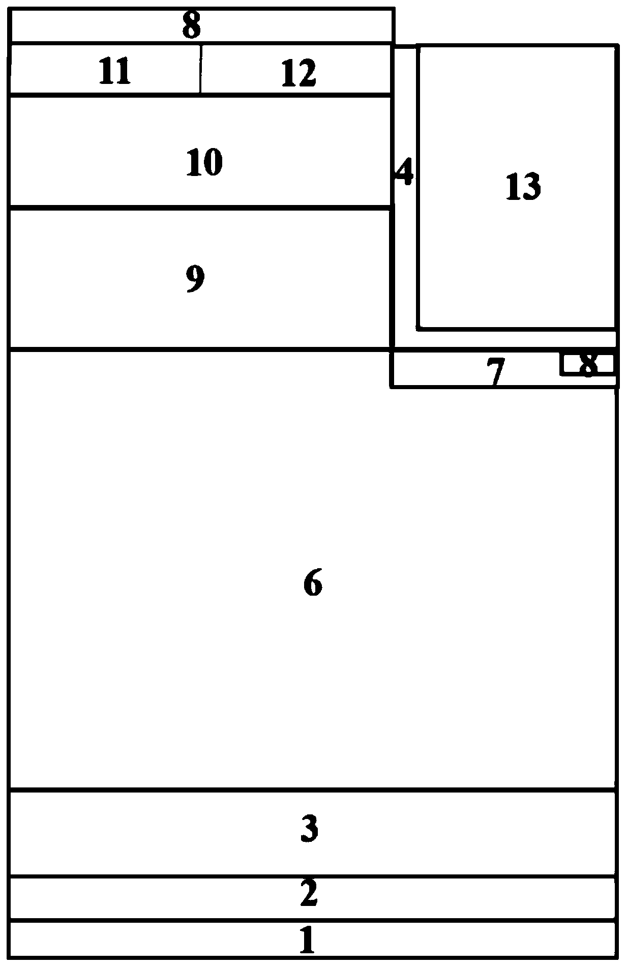
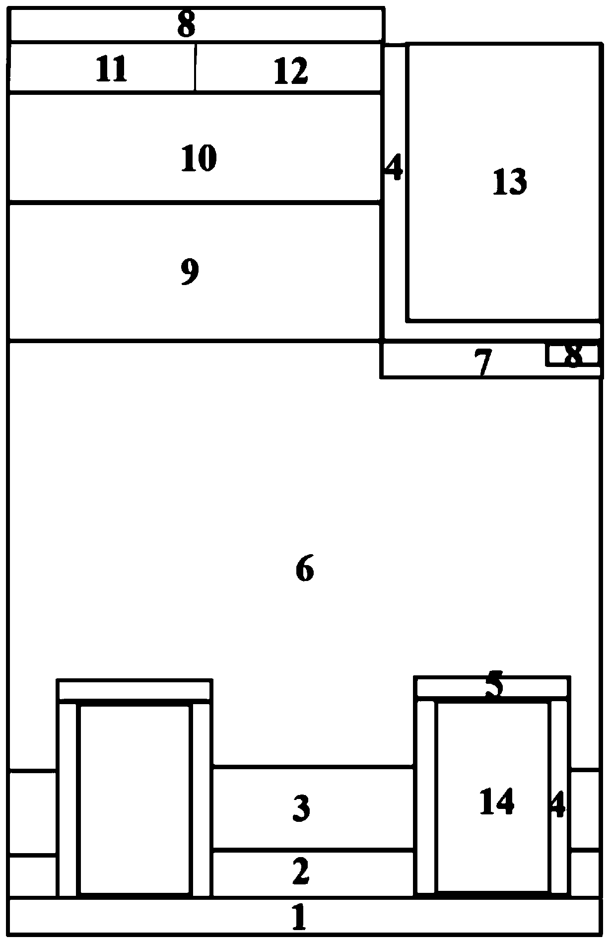
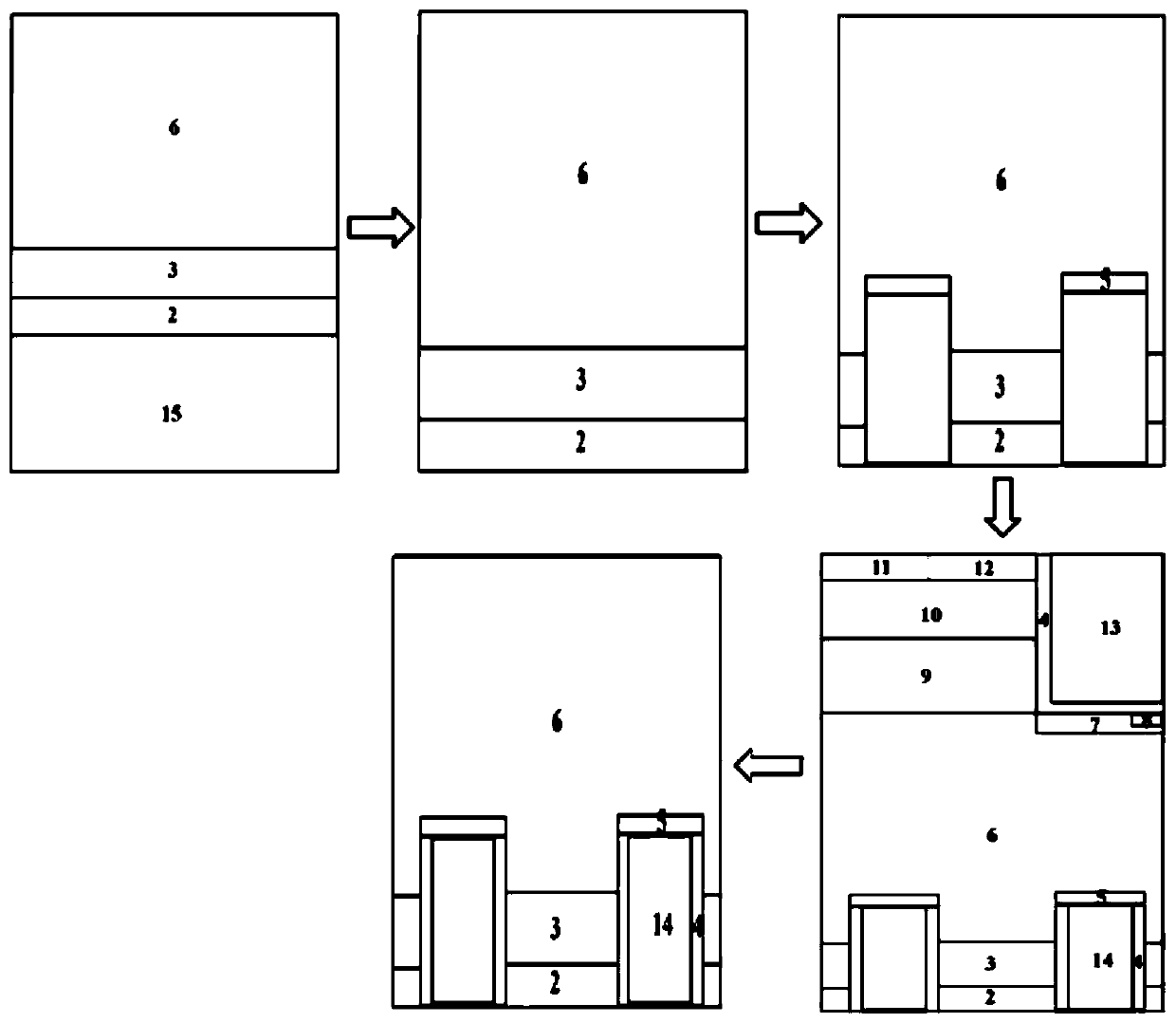
[0026] refer to Figure 1-4 , the present application provides a silicon carbide trench IGBT structure, including an N-type voltage barrier layer 6, a trench structure, and a trench collector metal electrode 14, a...


PUM

PropertyMeasurementUnit
Doping concentrationaaaaaaaaaa
Thicknessaaaaaaaaaa
Doping concentrationaaaaaaaaaa

Abstract

The invention discloses a silicon carbide trench IGBT structure, and the structure comprises an N-drift region, an N-type buffer layer, a P-type well region, a P+ ohmic contact region, an N+ emitter region, a P+ trench collector region, a trench collector, a P+ collector region, an N+ substrate layer, a trench gate and a gate oxide dielectric layer. Compared with a traditional structure, the structure is additionally provided with the trench collector on the collector, and is also additionally provided with the P+ trench collector above the trench collector; due to a fact that no N+ buffer layer is arranged above the P+ trench collector region of the new device, the hole injection efficiency during forward conduction is enhanced, and the turn-on voltage of the new device is reduced; when the new device is turned off, the trench collector provides a low-resistance channel, so the extraction of electrons is accelerated, and the turn-off loss is further reduced.

Description

technical field [0001] The invention relates to the technical field of insulated gate bipolar transistor devices, in particular to a high-voltage silicon carbide trench IGBT structure with a voltage greater than 15kV and a manufacturing method thereof. Background technique [0002] IGBTs is a composite tube composed of MOSFET and BJT, which combines the advantages of MOSFET and BJT, and is an ideal switching device. The excellent material properties of SiC, such as 3 times wider band gap, 10 times higher critical field strength, 3 times higher thermal conductivity and 2 times higher carrier saturation velocity, make SiC-based semiconductor devices widely used. The application of high temperature, high pressure, high power and other applications. In addition, since the characteristic on-resistance of unipolar devices is proportional to the 2.5th power of its breakdown voltage, SiC MOSFETs are not suitable for application in the field of breakdown voltage > 10kV. Due to t...

Claims


Application Information

Patent Timeline
IPC IPC(8): H01L29/06H01L29/08H01L29/739H01L21/331H01L21/28
CPCH01L29/7398H01L29/7397H01L29/66068H01L29/0684H01L29/0847H01L29/401Y02B70/10
Inventor 王颖苏芳文包梦恬于成浩曹菲李兴冀杨剑群吕钢
Owner 厦门吉顺芯微电子有限公司
Why Eureka
Try Eureka