Phase change memory unit and preparation method thereof

A phase-change memory and phase-change unit technology, applied in electrical components, semiconductor devices, electric solid-state devices, etc., can solve problems such as limited thermal budget, impact on device performance and yield, etc., to reduce device power consumption and achieve high density. The effect of storing and reducing the volume of the phase change operating area

Active Publication Date: 2020-05-12
SHANGHAI INTEGRATED CIRCUIT RES & DEV CENT
View PDF16 Cites 10 Cited by
  • Summary
  • Abstract
  • Description
  • Claims
  • Application Information

AI Technical Summary

Problems solved by technology

[0004]Figure The 3D X-point technology shown in 1 adopts the vertical stacking technology of two layers of phase change units to form high-density storage, but because the phase change material layer 04 in the phase change unit of the first layer is very sensitive to temperature, so When preparin

Method used


Image

  • Phase change memory unit and preparation method thereof
  • Phase change memory unit and preparation method thereof
  • Phase change memory unit and preparation method thereof

Examples


preparation example Construction

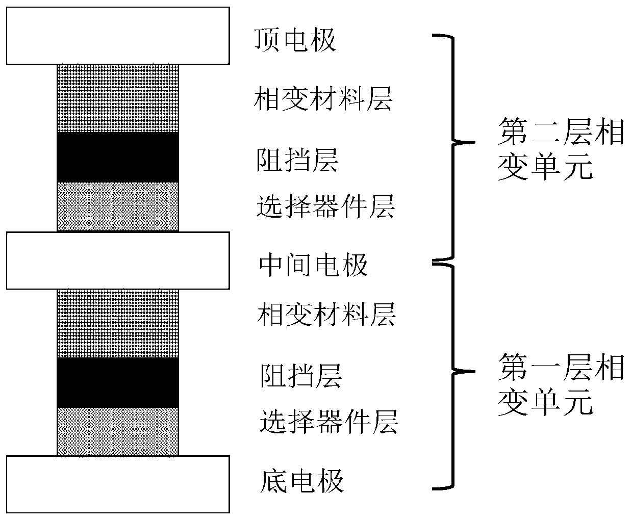
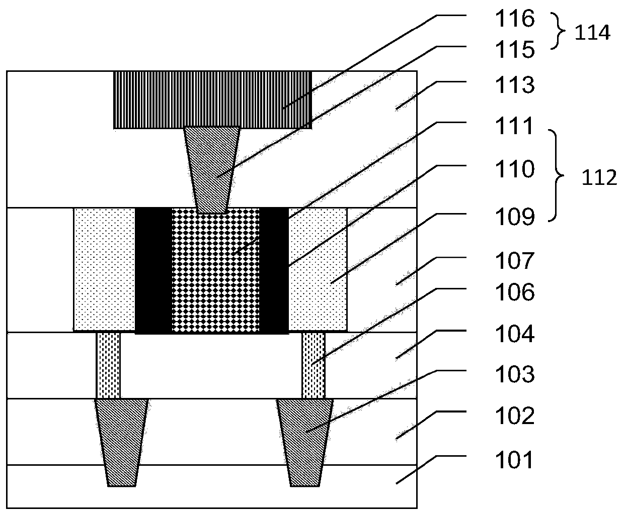
[0050] Please refer to Figure 3-Figure 9 , Figure 3-Figure 9 is prepared figure 2 A schematic diagram of the process steps of a phase-change memory cell structure. like Figure 3-Figure 9 As shown, a preparation method of a phase-change memory unit of the present invention may include the following steps:

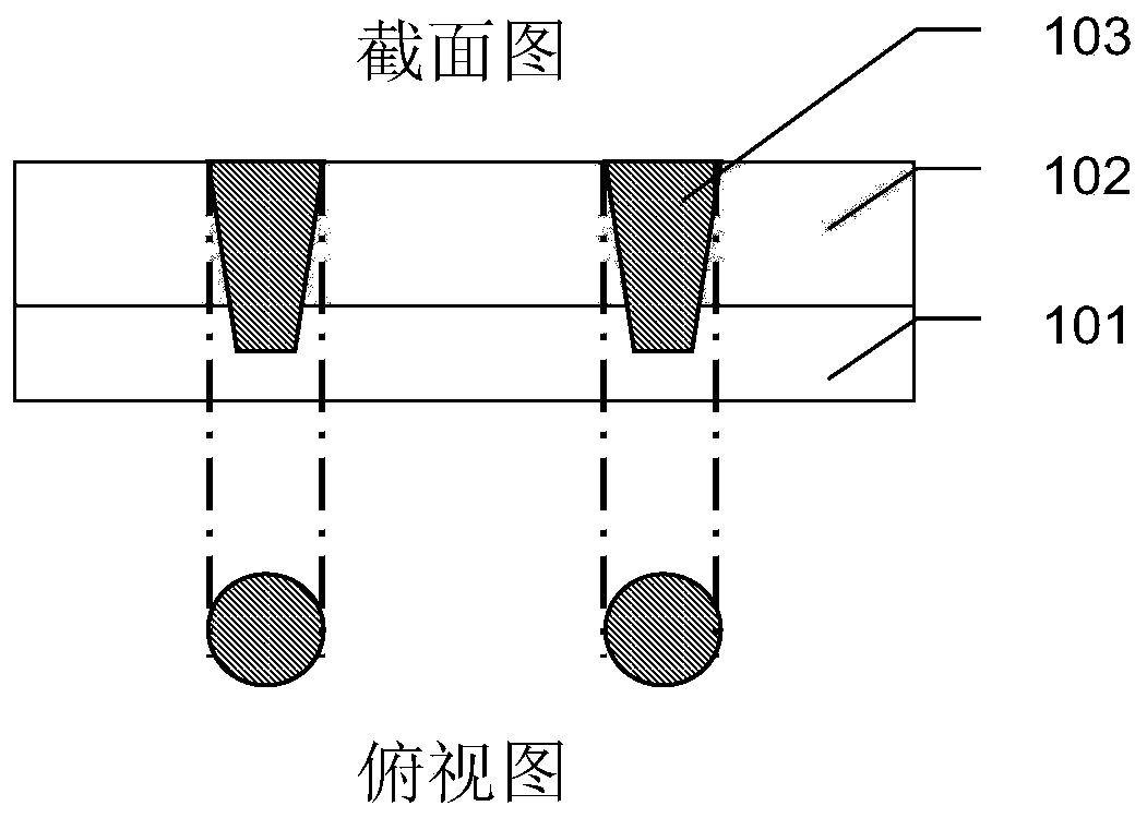
[0051] S11: If image 3 As shown, in order to clearly reflect the structure of the present invention, the upper figure in the figure shows a cross-sectional view, and the lower figure shows a top view (the same below), the first dielectric layer 102 is deposited on the substrate 101, and the substrate 101 and the first dielectric layer Two through-hole bottom electrodes 103 are formed in 102 .

[0052] Wherein, the lower half of the bottom electrode 103 can be located in the substrate 101 , and the upper half can be located in the first dielectric layer 102 . In this embodiment, the bottom electrode 103 may be a tungsten electrode through hole with a diameter of 40...


PUM


Abstract

The invention discloses a phase change memory unit. The phase change memory unit comprises bottom electrodes, heating electrodes, a phase change unit and a top electrode from bottom to top, and the phase change unit is of a longitudinally arranged cylinder structure and comprises a cylindrical selection device layer, an annular barrier layer and an annular phase change material layer from inside to outside; the plurality of bottom electrodes and the plurality of heating electrodes are in one-to-one correspondence, the bottom electrodes, the heating electrodes and the phase change material layer are sequentially connected, and the selection device layer is connected with the top electrode. According to the invention, the phase change unit and the plurality of heating electrodes are combinedtogether to form a structure that a plurality of phase change resistors share one selection device, and different phase change resistors can be connected with the bottom electrodes positioned on different metal interconnection layers through respective heating electrodes, so that the area of the chip in the horizontal direction is not increased, high-density storage is realized, the phase changematerial and the heating electrodes are very thin, and the power consumption of the device can be effectively reduced.

Description

technical field [0001] The invention relates to the technical field of semiconductor integrated circuit manufacturing technology, in particular to a high-density phase-change memory unit structure and a preparation method thereof. Background technique [0002] With the emergence of a series of new information technologies such as big data, the Internet of Things, cloud computing, and artificial intelligence, requirements for high read / write speed, low power consumption, high storage density, long service life, and high reliability have been put forward for memory. At present, new storage technologies represented by phase-change memory are gradually replacing traditional DRAM and Flash, and have broad application prospects in the fields of artificial intelligence and memory-computing integrated chips. [0003] The existing phase-change memory unit (taking Intel 3DX-point technology as an example) is composed of bottom electrode 01, selection device layer 02, barrier layer 03,...

Claims


Application Information

Patent Timeline
IPC IPC(8): H01L45/00H01L27/24
CPCH10B63/20H10N70/231H10N70/8418H10N70/8413H10N70/841H10N70/011
Inventor 钟旻冯高明李铭
Owner SHANGHAI INTEGRATED CIRCUIT RES & DEV CENT
Why Eureka
Try Eureka