Method for manufacturing a photoelectric semiconductor chip and bonding wafer used by method

A technology for optoelectronic semiconductors and chips, applied in the fields of semiconductor devices, semiconductor/solid-state device manufacturing, electric solid-state devices, etc., can solve problems such as crystal material waste, achieve good wavelength uniformity, and solve the effect of raw materials and chip processing costs.

Pending Publication Date: 2020-05-19
FUJIAN JING AN OPTOELECTRONICS CO LTD
View PDF8 Cites 0 Cited by
  • Summary
  • Abstract
  • Description
  • Claims
  • Application Information

AI Technical Summary

Problems solved by technology

The thicker the wafer is, the more cost is required to thin it in the chip manufacturing process, which is a lot of waste of crystal material

Method used


Image

  • Method for manufacturing a photoelectric semiconductor chip and bonding wafer used by method
  • Method for manufacturing a photoelectric semiconductor chip and bonding wafer used by method
  • Method for manufacturing a photoelectric semiconductor chip and bonding wafer used by method

Examples


Embodiment Construction

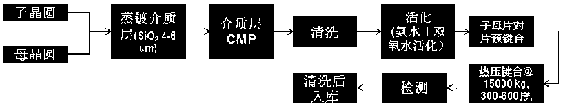
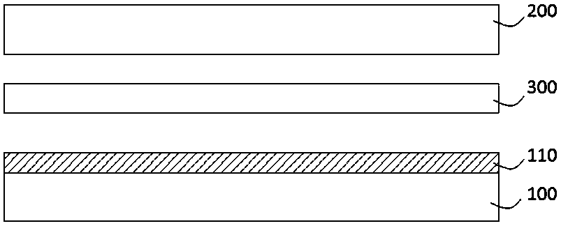
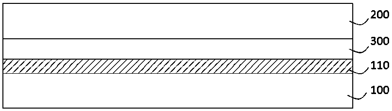
[0024] Several specific embodiments of the present invention will be further described in detail below with reference to the accompanying drawings. However, the following descriptions and explanations about the embodiments do not constitute any limitation to the protection scope of the present invention.

[0025] It should be understood that the terminology used in the present invention is for the purpose of describing specific embodiments only, and is not intended to limit the present invention. It is further understood that when the terms "comprising" and "comprising" are used in the present invention, they are intended to indicate the presence of stated features, integers, steps, components, without excluding one or more other features, integers, steps, components and / or or the presence or increase of their combination.

[0026] Unless otherwise defined, all terms (including technical and scientific terms) used in the present invention have the same meaning as commonly und...


PUM

PropertyMeasurementUnit
thicknessaaaaaaaaaa
thicknessaaaaaaaaaa
thicknessaaaaaaaaaa

Abstract

The invention provides a method for manufacturing a photoelectric semiconductor chip and a bonding wafer used by the method. Wafer materials comprise sapphire, silicon carbide, gallium arsenide and other wafers used for epitaxy (epitaxy). According to the method, a traditional wafer is divided into a mother wafer and a child wafer, and after the mother wafer and the child wafer are bonded by usinga proper bonding technology, the warping change generated by high temperature and stress at about 1000 DEG C during epitaxy can be resisted; and after epitaxy, the bonding is released by using a non-physical damage mode. The mother wafer can be recycled, the son wafer and the epitaxial layer are directly used for the chip manufacturing process, thinning or little thinning is not needed, the problem of raw material and chip machining cost of a large-size epitaxial wafer is solved, and an epitaxial wafer with better wavelength uniformity is obtained.

Description

technical field [0001] The invention relates to a manufacturing method of an optoelectronic semiconductor chip, in particular to a bonding wafer suitable for epitaxy. Background technique [0002] Single crystal sapphire, silicon carbide, and gallium arsenide crystals are typical epitaxial materials with excellent photoelectric effect, and are widely used in LEDs and power devices. Crystals such as sapphire, silicon carbide, and gallium arsenide consume a lot of electricity when growing. And the larger the wafer size, the lower the yield of the crystal material, the semiconductor substrate wafer gradually transitions from 4 inches to 6 inches or 8 inches, and the cost is relatively high. [0003] The crystal needs to undergo multiple processes such as cutting, grinding, polishing, and cleaning to become a wafer; after epitaxial growth, the chip manufacturing process needs to reduce the thickness of the entire chip to reduce the size of the chip. The thickness of the chip i...

Claims


Application Information

Patent Timeline
Patent Type & Authority Applications(China)
IPC IPC(8): H01L21/683H01L33/00H01L33/44
CPCH01L21/6835H01L33/44H01L33/005H01L2221/68345H01L2933/0025H01L33/0093H01L21/02293
Inventor 谢斌晖陈铭欣萧尊贺郑贤良宋志棠刘卫丽
Owner FUJIAN JING AN OPTOELECTRONICS CO LTD
Why Eureka
Try Eureka