Mismatch-free II-type superlattice structure based on antimony shutter switch and preparation method

A shutter switch, superlattice technology, applied in the direction of final product manufacturing, sustainable manufacturing/processing, ion implantation plating, etc., can solve problems such as complex process, and achieve the effect of simplifying process steps, reducing complexity, and improving purity

Pending Publication Date: 2020-06-02
中科爱毕赛思(常州)光电科技有限公司
View PDF0 Cites 0 Cited by
  • Summary
  • Abstract
  • Description
  • Claims
  • Application Information

AI Technical Summary

Problems solved by technology

[0006] 2. The problem of complex process when the InSb interface layer is directly epitaxially grown;

Method used


Image

  • Mismatch-free II-type superlattice structure based on antimony shutter switch and preparation method
  • Mismatch-free II-type superlattice structure based on antimony shutter switch and preparation method

Examples


Embodiment 1

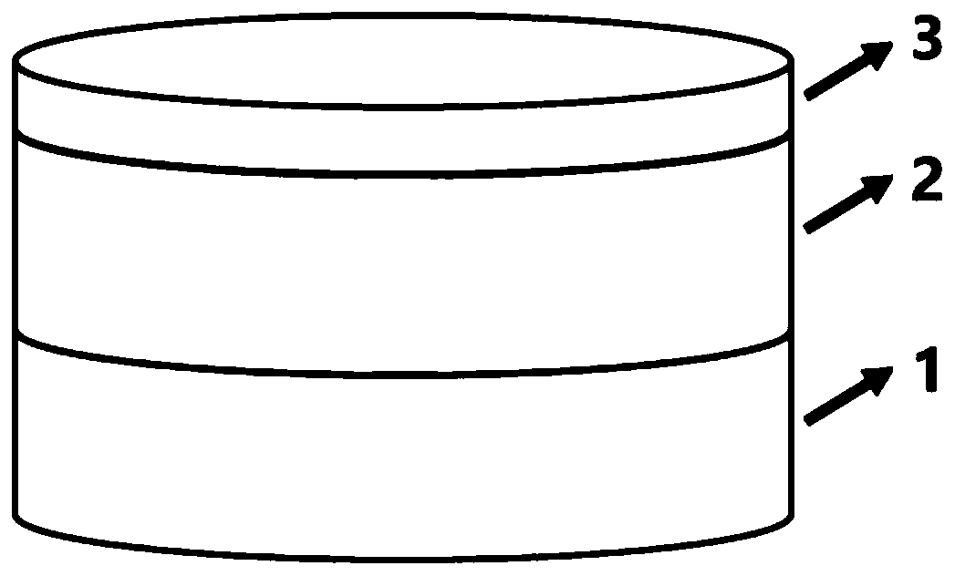
[0022] According to the content of the invention, we have prepared a type II superlattice material, the specific structure of which is:

[0023] The thickness of GaSb layer 1 is 1.05nm;

[0024] The thickness of the InAs layer 2 is 2.45nm;

[0025] InAs x Sb 1-x Layer 3 has a thickness of 0.3 nm and a composition x of 0.20;

[0026] Its specific preparation method is:

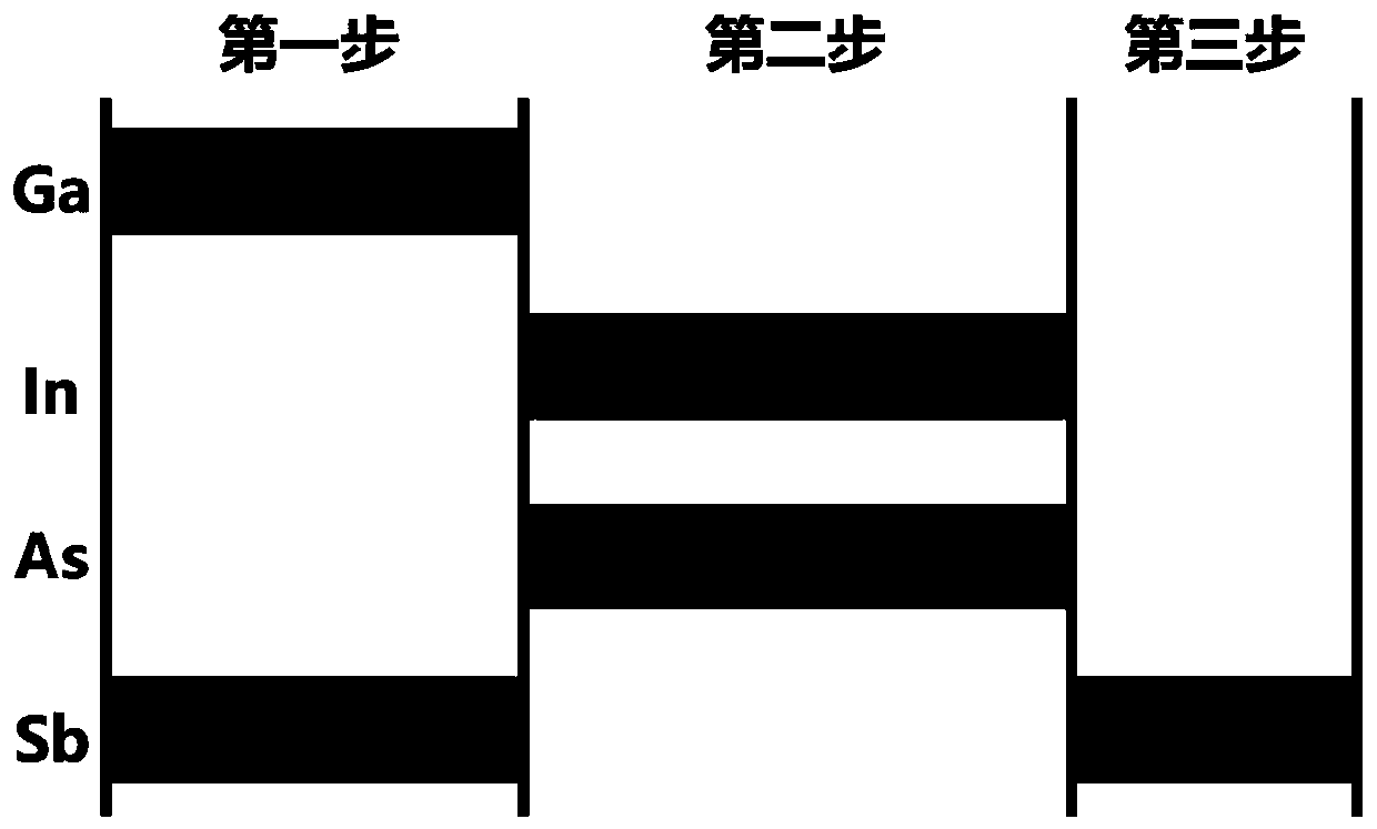
[0027] 1) The GaSb substrate is heated up to the deoxidation temperature, and the oxide layer on the surface is removed under the protection of the Sb beam. The deoxidation temperature is 560 °C, and the Sb beam is 2×10 -6 Torr;

[0028] 2) Cool down the GaSb substrate to the type II superlattice growth temperature of 395°C;

[0029] 3) Set the As / In and Sb / Ga growth beam current ratios to 4 and 5, respectively;

[0030] 4) Using molecular beam epitaxy to grow InAs / GaSb II superlattice on the GaSb substrate, the first step is to open the Ga and Sb shutters to epitaxially GaSb layer 1, and the second step...

Embodiment 2

[0032] According to the content of the invention, we have prepared a type II superlattice material, the specific structure of which is:

[0033] GaSb layer 1 has a thickness of 2.1 nm;

[0034] The thickness of the InAs layer 2 is 1.2nm;

[0035] InAs x Sb 1-x The thickness of layer 3 is 0.3nm, the component x is 0.39, and the Sb infiltration time is 1s;

[0036] Its specific preparation method is:

[0037] 1) The GaSb substrate is heated up to the deoxidation temperature, and the oxide layer on the surface is removed under the protection of the Sb beam. The deoxidation temperature is 570°C, and the Sb beam is 2×10 -6 Torr;

[0038] 2) Cool down the GaSb substrate to the type II superlattice growth temperature of 400°C;

[0039] 3) Set the As / In and Sb / Ga growth beam current ratios to 4 and 5, respectively;

[0040] 4) Using molecular beam epitaxy to grow InAs / GaSb II superlattice on the GaSb substrate, the first step is to open the Ga and Sb shutters to epitaxially GaS...

Embodiment 3

[0042] According to the content of the invention, we have prepared the third type II superlattice material, the specific structure of which is:

[0043] The thickness of the GaSb layer 1 is 2.4nm;

[0044] The thickness of the InAs layer 2 is 3.0nm;

[0045] InAs x Sb 1-x Layer 3 has a thickness of 0.3 nm and a composition x of 0.02;

[0046] Its specific preparation method is:

[0047] 1) The GaSb substrate is heated up to the deoxidation temperature, and the oxide layer on the surface is removed under the protection of the Sb beam. The deoxidation temperature is 580°C, and the Sb beam is 2×10 -6 Torr;

[0048] 2) Cool down the GaSb substrate to the type II superlattice growth temperature of 405°C;

[0049] 3) Set the As / In and Sb / Ga growth beam current ratios to 4 and 5, respectively;

[0050] 4) Using molecular beam epitaxy to grow InAs / GaSb II superlattice on the GaSb substrate, the first step is to open the Ga and Sb shutters to epitaxially GaSb layer 1, and the seco...


PUM

PropertyMeasurementUnit
thicknessaaaaaaaaaa
thicknessaaaaaaaaaa
thicknessaaaaaaaaaa

Abstract

The invention discloses a mismatch-free II-type superlattice structure based on an antimony shutter switch and a preparation method. The single-cycle structure comprises a three-layer structure of a GaSb layer, an InAs layer and an InAsSb interface layer. The preparation method comprises the steps of in the growth process of the II-type superlattice periodic structure, directly growing the InAs layer after GaSb growth, opening an Sb shutter after InAs growth, and enabling Sb and As in the InAs layer to be subjected to element replacement so as to form the InAsSb interface layer. The method ischaracterized in that the direct growth of the InSb interface layer is cancelled; the InAsSb interface layer is formed only by introducing Sb infiltration after InAs growth, so that the requirement ofstress compensation is met, and the difficulty of an interface preparation process is simplified. In addition, the defect of an island-mounted structure introduced during direct growth of a large-mismatch InSb interface is avoided, and the material performance is improved.

Description

technical field [0001] The invention relates to a superlattice material, in particular to a non-mismatch II type superlattice structure based on an antimony shutter switch and a preparation method thereof, which is applied to an infrared focal plane detector. Background technique [0002] In the early 1970s, scientists L.Esaki and Sakaki of the IBM laboratory proposed the concept of the InAs / GaSb II superlattice, and then, in the late 1980s, Smith and Maihiot proposed that the InAs / GaSb II superlattice can be applied to The idea of ​​infrared detection technology. The InAs / GaSb II superlattice can realize the adjustment of the detection wavelength from 3 μm to 30 μm by changing the thickness of the InAs and GaSb layers. It is the preferred material system for the preparation of a new generation of high-performance infrared detectors. Based on the many theoretical advantages and characteristics of superlattice in the application of infrared detectors, research institutions a...

Claims


Application Information

Patent Timeline
Patent Type & Authority Applications(China)
IPC IPC(8): H01L31/0352H01L31/18C23C14/02C23C14/06
CPCC23C14/0021C23C14/02C23C14/0617H01L31/035236H01L31/1844Y02P70/50
Inventor 徐志成朱艺红梁钊铭陈凯豪陈建新
Owner 中科爱毕赛思(常州)光电科技有限公司
Why Eureka
Try Eureka