Schottky diode with high-phosphorus-doped N-type cut-off ring structure and preparation method

A technology of Schottky diodes and cut-off rings, which is applied in semiconductor/solid-state device manufacturing, electrical components, circuits, etc., can solve problems such as inability to eliminate pollution and increase manufacturing costs, and achieve low manufacturing costs and improved high-temperature aging performance.

Pending Publication Date: 2020-06-19
桑德斯微电子器件(南京)有限公司
View PDF4 Cites 0 Cited by
  • Summary
  • Abstract
  • Description
  • Claims
  • Application Information

AI Technical Summary

Problems solved by technology

However, the current Schottky diode structure is basically a P-type protective ring in the active area, and silicon dioxide is used as the dielectric layer on the outer edge; only by controlling the cleanliness or improving the packaging material and sealing, it is impossible to eliminate artificial Pollution caused, but also increase manufacturing costs, not feasible

Method used


Image

  • Schottky diode with high-phosphorus-doped N-type cut-off ring structure and preparation method
  • Schottky diode with high-phosphorus-doped N-type cut-off ring structure and preparation method
  • Schottky diode with high-phosphorus-doped N-type cut-off ring structure and preparation method

Examples


Embodiment Construction

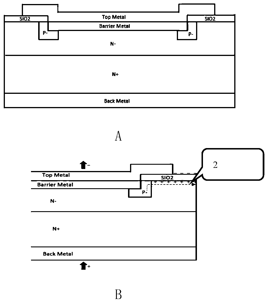
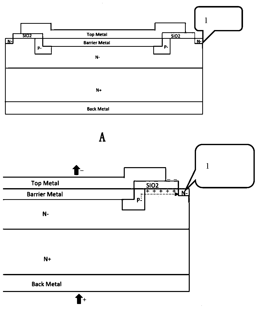
[0024] Such as figure 2 , a schematic diagram of the operation of the high-voltage Schottky diode of the present invention after adding a cut-off ring. Ion implantation is performed on the edge of the oxide layer of the N-type semiconductor to produce a high-concentration N-type semiconductor on the surface, and the ion beam is phosphorus ions.

[0025] Schottky diodes, with N-type semiconductors as the substrate, an N-epitaxial layer is formed on the substrate, and the anode on the N-epitaxial layer is made of molybdenum or aluminum as a barrier layer; high-voltage Schottky diodes may have a P-type protection ring. Such as figure 2 shown.

[0026] ①The specific position of the depletion layer of the high-voltage Schottky diode outside the step of the contact hole is simulated by the device simulation software, mainly to confirm the position of the front metal edge, so as to prevent the reverse breakdown voltage from being too short. Low (need to consider the amount of w...


PUM


Abstract

A Schottky diode with a high-phosphorus-doped N-type cut-off ring structure is characterized in that an N-type semiconductor is used as a substrate, an N-epitaxial layer is formed on the substrate, ananode is arranged on the N-epitaxial layer, and a blocking layer is made of molybdenum or aluminum and other materials. The diode is characterized in that phosphorus ions are injected into a Schottkydiode scribing channel. The cut-off ring is designed inside or outside the scribing channel, and the width of the cut-off ring is larger than that of the original scribing channel. Phosphorus ion implantation is arranged after the cut-off ring is corroded, at the moment, except that the cut-off ring is opened, other parts of the surface are all covered with photoresist, and the phosphorus ion implantation reaches the maximum concentration on the surface of the semiconductor.

Description

technical field [0001] The invention relates to a schottky diode device, especially the improvement of high-voltage (above 100V) schottky diode aging characteristics at high temperature. Background technique [0002] As we all know, SBD is the abbreviation of Schottky Barrier Diode (Schottky Barrier Diode, abbreviated as SBD). SBD is not made by the principle of contacting P-type semiconductor and N-type semiconductor to form PN junction, but by using the principle of metal-semiconductor junction formed by contacting metal and semiconductor. Therefore, SBD is also called metal-semiconductor (contact) diode or surface barrier diode; Schottky diode has low reverse breakdown voltage and reverse leakage due to its own special characteristics-noble metal and N-type semiconductor structure. great features. However, with market demand and technology updates, Schottky diodes currently have a reverse breakdown voltage of 200V and above, and are used in mobile phones, automobiles, m...

Claims


Application Information

Patent Timeline
IPC IPC(8): H01L29/06H01L29/872H01L21/329
CPCH01L29/872H01L29/66143H01L29/0638H01L29/0684
Inventor 胡明辉杨敏红单慧刘韵吉
Owner 桑德斯微电子器件(南京)有限公司
Why Eureka
Try Eureka