Readout circuit structure and working time sequence control method thereof

A readout circuit and reset control technology, which is applied in TV, electrical components, color TV, etc., can solve the problems of complex timing control of the readout circuit, loss of analog signal input, large area occupied by capacitors, etc., so as to improve chip cost Competitiveness, improved circuit accuracy, and reduced complexity

Active Publication Date: 2020-06-23
SHANGHAI INTEGRATED CIRCUIT RES & DEV CENT +1
View PDF5 Cites 2 Cited by
  • Summary
  • Abstract
  • Description
  • Claims
  • Application Information

AI Technical Summary

Problems solved by technology

Although this structure can achieve offset elimination and improve circuit accuracy, it needs to add at least 5 switches and 2 capacitors, such as image 3 The five switches of PGA_OS1, PGA_OS2, OS_C1, OS_C1N, and OS_C2 and the two capacitors of Cc and Cc2
Therefore, there are the following three problems in this structure: (1) Since the realization of the capacitor in the CMOS process occupies a relatively large area, increasing the two capacitors Cc and Cc2 will inevitably lead to a large total area to be occupied; (2) ) When the ADC performs analog-to-digital conversion, the parasitic capacitance Cp at the input terminal of the comparator COMP will form a capacitive voltage divider structure with the offset storage capacitor Cc2, so that the actual analog signal input of the ADC will be multiplied by Cc2 / (Cc2+Cp) this coefficient, which is obviously less than 1, that is, the actual analog signal input of the ADC is lost; (3) due to the increased number of switches, the control signal also increases correspondingly, which will cause the timing control of the readout circuit to be more complicated. like Figure 4 as shown, Figure 4 Yes image 3 The schematic diagram of the working timing of the readout circuit structure with the offset cancellation function shown, the entire circuit working timing cycle of the readout circuit structure can include the offset cancellation working phase and the normal programmable gain amplifier circuit and analog-to-digital converter circuit working phase (that is, the normal PGA+ADC working phase) these two phases
[0007] Therefore, it is necessary to propose a new readout circuit structure, so that the readout circuit structure can reduce the use of capacitors and switches while having the function of offset elimination, so as to save area and power consumption, reduce the timing complexity of control signals, and avoid Accuracy loss of existing structures to improve accuracy

Method used


Image

  • Readout circuit structure and working time sequence control method thereof
  • Readout circuit structure and working time sequence control method thereof
  • Readout circuit structure and working time sequence control method thereof

Examples


Embodiment Construction

[0037] In order to make the purpose, advantages and characteristics of the present invention clearer, the following in conjunction with the attached Figure 5-7 The structure of the readout circuit proposed by the present invention and its working sequence control method are further described in detail. It should be noted that all the drawings are in a very simplified form and use imprecise scales, and are only used to facilitate and clearly assist the purpose of illustrating the embodiments of the present invention.

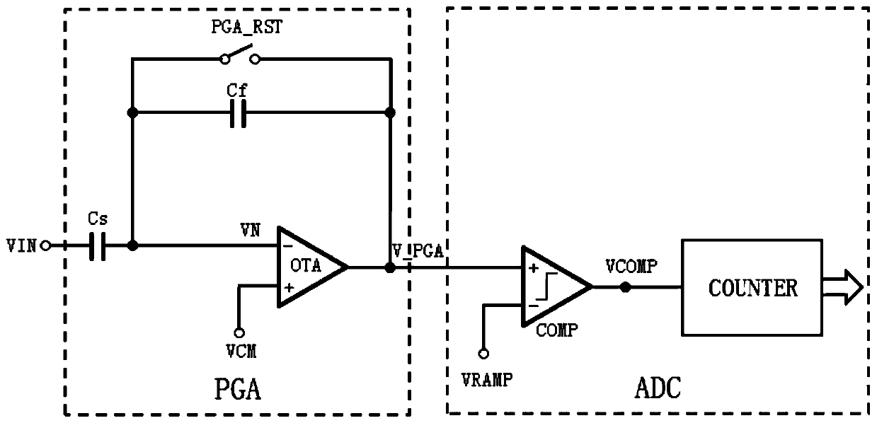
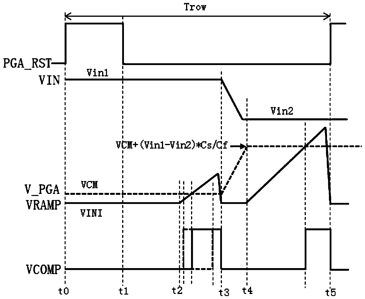
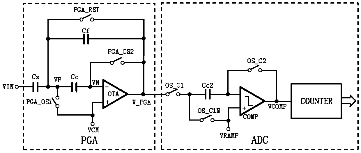
[0038] An embodiment of the present invention provides a readout circuit structure, refer to Figure 5 , Figure 5 It is a schematic diagram of the structure of a readout circuit with an offset cancellation function according to an embodiment of the present invention, from Figure 5 It can be seen that the readout circuit structure includes: a programmable gain amplifier circuit PGA and an analog-to-digital converter circuit ADC provided by phase coupling, and...


PUM


Abstract

The invention provides a readout circuit structure and a working time sequence control method thereof. The readout circuit structure comprises a programmable gain amplifier circuit and an analog-to-digital converter circuit which are arranged in a coupling mode, the programmable gain amplifier circuit comprises a sampling capacitor, a feedback capacitor, an operational amplifier and a reset control switch, and the analog-to-digital converter circuit comprises a comparator and a counter. Wherein one end of the reset control switch is connected with one input end of the operational amplifier, the other end of the reset control switch is connected with the output end of the comparator, the output end of the operational amplifier is connected with one input end of the comparator, and the otherinput end of the comparator is connected with a reference voltage. According to the technical scheme, the readout circuit structure has an offset elimination function, and meanwhile, the use of capacitors and switches can be reduced, so that the area and the power consumption are saved, the time sequence complexity of control signals is reduced, and the overall circuit precision is improved.

Description

technical field [0001] The invention relates to the technical field of integrated circuits, in particular to a readout circuit structure and a working sequence control method thereof. Background technique [0002] In CIS (CMOS Image Sensor, CMOS image sensor), it is usually necessary to convert the light signal into a voltage signal in the photosensitive unit (pixel) and then connect the PGA (Programmable Gain Amplifier, programmable gain amplifier) ​​to amplify the voltage signal, and then connect the ADC (Analog Digital Converter (analog-to-digital converter) circuit converts the analog voltage signal into a digital signal, and finally transmits the converted digital signal to the outside of the chip. Since the photosensitive units are usually in the form of an array, in order to increase the frame rate, usually each column of photosensitive units is connected to a column of readout circuits composed of PGA and ADC. [0003] refer to figure 1 , figure 1 is a schematic d...

Claims


Application Information

Patent Timeline
Patent Type & Authority Applications(China)
IPC IPC(8): H04N5/378H04N5/374
CPCH04N25/76H04N25/75
Inventor 何学红杨海玲董林妹李志芳黄耀
Owner SHANGHAI INTEGRATED CIRCUIT RES & DEV CENT
Why Eureka
Try Eureka