LED epitaxial structure, manufacturing method thereof and LED chip

A technology of epitaxial structure and manufacturing method, applied in the direction of electrical components, circuits, semiconductor devices, etc., can solve problems affecting LED luminous efficiency, lattice mismatch, etc., achieve high luminous efficiency, less electron leakage, and reduce stress mismatch Effect

Active Publication Date: 2020-06-26
XIAMEN QIANZHAO SEMICON TECH CO LTD
View PDF4 Cites 5 Cited by
  • Summary
  • Abstract
  • Description
  • Claims
  • Application Information

AI Technical Summary

Problems solved by technology

However, there will be a lattice mismatch between the InGaN quantum well and the GaN quantum barrier, which will cause polarization, which will bend the energy band of the MQWs region, and ultimately affect the luminous efficiency of the LED.

Method used


Image

  • LED epitaxial structure, manufacturing method thereof and LED chip
  • LED epitaxial structure, manufacturing method thereof and LED chip
  • LED epitaxial structure, manufacturing method thereof and LED chip

Examples


Embodiment 1

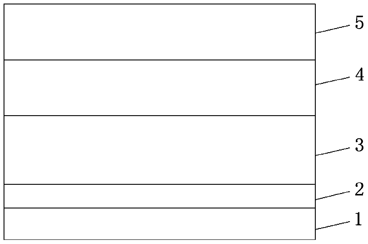
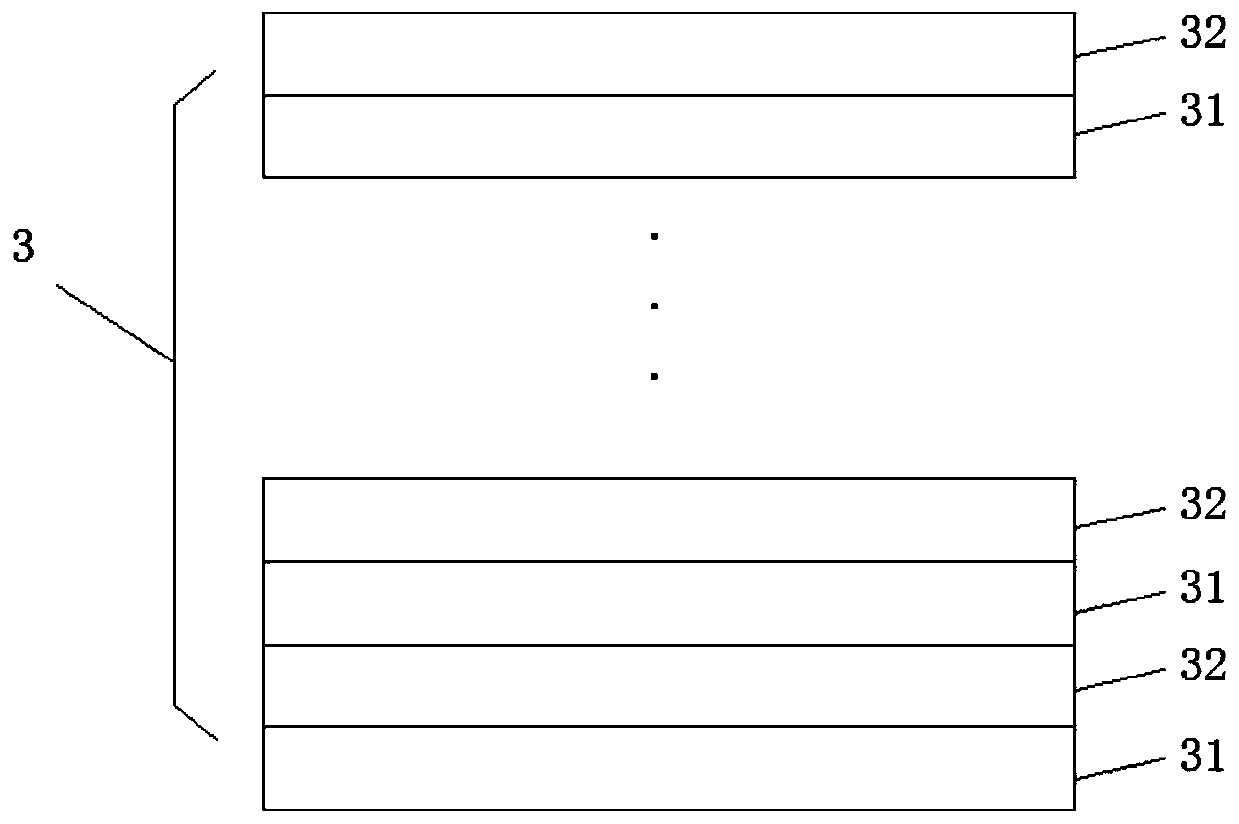
[0059] An LED epitaxial structure, including a substrate 1, a buffer layer 6, an undoped GaN layer 7, a first-type semiconductor layer 2, a multi-quantum well barrier layer 3, an electron blocking layer 4, and a second-type semiconductor layer 5 stacked in sequence , the multiple quantum well barrier layer 3 includes a quantum well 31 and a quantum barrier 32, wherein the buffer layer 6 is a GaN buffer layer, the first semiconductor layer 2 is an N-type GaN layer doped with Si, and the electron barrier Layer 4 is a P-type electron blocking layer, and the second-type semiconductor layer 5 is a P-type GaN layer. Please refer to figure 1 and figure 2 .

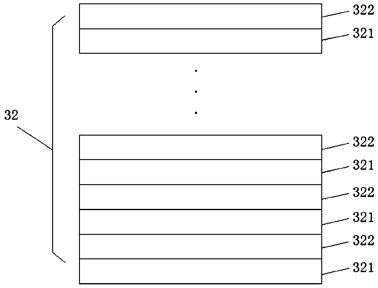
[0060] Please refer to image 3 , the quantum barrier 32 is an AlInGaN / AlGaN superlattice structure, the period of the AlInGaN / AlGaN superlattice structure is multiple, each period includes an AlInGaN layer 321 and an AlGaN layer 322, and the Al group of the AlInGaN layer 321 Minutes change as the number of periods increases...

Embodiment 2

[0064] An LED epitaxial structure, the difference from the first embodiment above is that the thickness of the AlInGaN / AlGaN superlattice structure decreases as the number of periods increases, please refer to Figure 7 . Wherein, the abscissa refers to the AlInGaN / AlGaN superlattice structure, and the ordinate refers to the thickness of the AlInGaN / AlGaN superlattice structure.

Embodiment 3

[0066] An LED epitaxial structure, the difference from the second embodiment above is that the AlInGaN / AlGaN superlattice structure has Si doping, and the change of Si doping concentration includes but not limited to: with the period of the AlInGaN / AlGaN superlattice structure increase or decrease gradually. Please refer to the specific change diagram Figure 8a and Figure 8b , where the abscissa refers to the AlInGaN / AlGaN superlattice structure, and the ordinate refers to the Si doping concentration of the AlInGaN / AlGaN superlattice structure. It should be noted, Figure 8a and Figure 8b It is only for illustration and not for limitation of the present invention.


PUM


Abstract

The invention provides an LED epitaxial structure, a manufacturing method thereof and an LED chip. The epitaxial structure comprises a substrate, a first type semiconductor layer, a multi-quantum wellbarrier layer, an electron blocking layer and a second type semiconductor layer which are stacked in sequence. The multi-quantum well barrier layer comprises a quantum well and a quantum barrier, andthe quantum barrier is of an AlInGaN/AlGaN superlattice structure. The AlInGaN/AlGaN superlattice structure has a plurality of periods, each period comprises an AlInGaN layer and an AlGaN layer, andthe Al component of the AlInGaN layer is changed along with the increase of the number of periods so as to be matched with the polarization of the quantum well. The quantum barrier adopts an AlInGaN/AlGaN superlattice structure, so that the stress mismatch between the quantum well and the quantum barrier can be reduced, the polarization electric field can be reduced, and the electron leakage caused by the bending of the energy band of the quantum well can be reduced. Meanwhile, polarization matching with the quantum well is realized by adjusting the Al component.

Description

technical field [0001] The invention relates to the field of light-emitting diodes, in particular to an LED epitaxial structure, a manufacturing method thereof, and an LED chip. Background technique [0002] Group III-V compounds are known as the third-generation semiconductor materials, among which nitrides are widely used in blue and green light-emitting diodes due to their wide band gap, high electron mobility, high luminous efficiency, and high frequency. , lasers and other semiconductor devices. [0003] In the MQWs layer structure of the traditional epitaxial wafer, the quantum well is composed of InGaN, and the quantum barrier is composed of GaN. However, there will be a lattice mismatch between the InGaN quantum well and the GaN quantum barrier, which will cause polarization, which will bend the energy band of the MQWs region, and ultimately affect the luminous efficiency of the LED. Contents of the invention [0004] In view of this, the purpose of the present i...

Claims


Application Information

Patent Timeline
Patent Type & Authority Applications(China)
IPC IPC(8): H01L33/04H01L33/06H01L33/12H01L33/14H01L33/32H01L33/00
CPCH01L33/0075H01L33/04H01L33/06H01L33/12H01L33/145H01L33/32
Inventor 蔺宇航卓祥景尧刚程伟林志伟
Owner XIAMEN QIANZHAO SEMICON TECH CO LTD
Why Eureka
Try Eureka