Monocrystalline silicon ingot and preparation method thereof, cast monocrystalline silicon wafer and preparation method for cast monocrystalline silicon wafer

A technology of monocrystalline silicon ingots and monocrystalline silicon wafers, which is applied in the field of silicon wafers to achieve the effect of reducing production costs, low production costs, and favorable application

Inactive Publication Date: 2020-07-03
JIANGSU XIEXIN SILICON MATERIAL TECH DEV
View PDF4 Cites 1 Cited by
  • Summary
  • Abstract
  • Description
  • Claims
  • Application Information

AI Technical Summary

Problems solved by technology

[0004] Based on this, it is necessary to provide a low-cost monocrystalline silicon ingot and its preparation method, cast monocrystalline silicon wafer and its preparation method for the problem of how to reduce costs

Method used


Image

  • Monocrystalline silicon ingot and preparation method thereof, cast monocrystalline silicon wafer and preparation method for cast monocrystalline silicon wafer
  • Monocrystalline silicon ingot and preparation method thereof, cast monocrystalline silicon wafer and preparation method for cast monocrystalline silicon wafer
  • Monocrystalline silicon ingot and preparation method thereof, cast monocrystalline silicon wafer and preparation method for cast monocrystalline silicon wafer

Examples


preparation example Construction

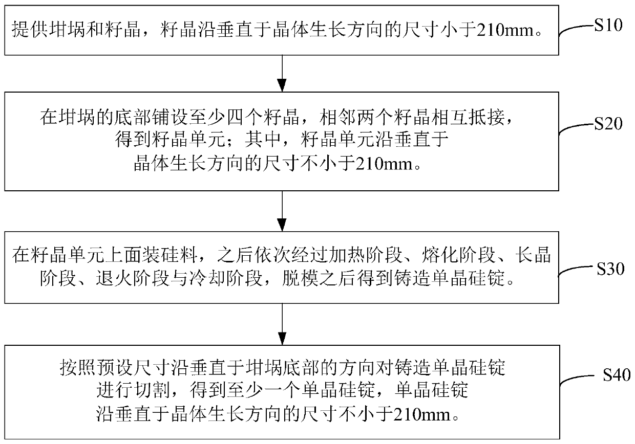
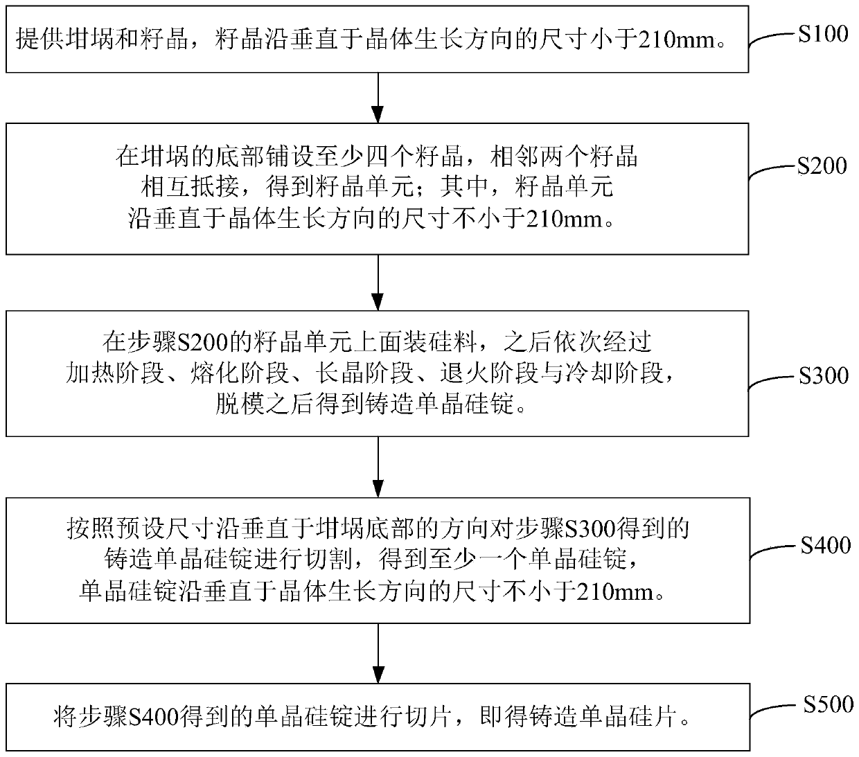
[0043] See figure 1 , The method for preparing a single crystal silicon ingot according to an embodiment of the present invention includes the following steps:

[0044] S10. Provide a crucible and a seed crystal, and the size of the seed crystal along the direction perpendicular to the crystal growth direction is less than 210mm.

[0045] Among them, the crucible is a crucible of polycrystalline silicon or single crystal silicon commonly used in the field, such as a quartz crucible.

[0046] Among them, the seed crystal is a small crystal with the same crystal orientation as the desired crystal, and is the seed for growing a single crystal, also called a seed crystal. The seed crystal is usually obtained by Czochralski. The size of the seed crystal along the direction perpendicular to the crystal growth direction is less than 210 mm means that the length of any side of the seed crystal along the direction perpendicular to the crystal growth direction is less than 210 mm. Wherein, th...

Embodiment 1

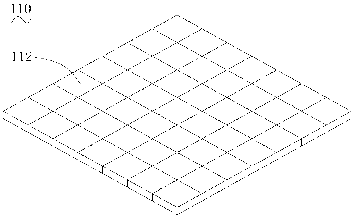
[0090] See image 3 The seed crystal unit 110 of an embodiment includes 49 square seed crystals 112 arranged in rows and columns, and adjacent seed crystals 112 are closely arranged. Wherein, the length and width of each seed crystal 112 are both 150 mm, and the number of seed crystals 112 in each row and column is 7 each.

[0091] The silicon material is loaded on the seed crystal unit 110, and then goes through the heating stage, the melting stage, the crystal growth stage, the annealing stage and the cooling stage. After demolding, a cast single crystal silicon ingot 120 is obtained. The weight of the cast single crystal silicon ingot 120 is approximately 1100Kg, such as Figure 4 Shown.

[0092] Figure 4 The middle dashed line is the cutting line. The cast single crystal silicon ingot 120 is cut along the cutting line to obtain 25 single crystal silicon ingots 122. Among them, the cutting lines include four transversely and four longitudinally, and the four transversely cutti...

Embodiment 2

[0096] See Image 6 The seed crystal unit 210 of Embodiment 2 includes 25 square seed crystals 212 arranged in rows and columns, and adjacent seed crystals 212 are closely arranged. The length and width of each seed crystal 212 are both 156 mm, and the number of seed crystals 212 in each row and column is 5.

[0097] The silicon material is loaded on the seed crystal unit 210, and then the heating phase, the melting phase, the crystal growth phase, the annealing phase and the cooling phase are successively passed through. After demolding, a cast single crystal silicon ingot 220 is obtained. The weight of the cast single crystal silicon ingot 220 is approximately 850Kg, such as Figure 7 Shown.

[0098] Figure 7 The middle dashed line is the cutting line. The cast single crystal silicon ingot 220 is cut along the cutting line to obtain 16 single crystal silicon ingots 222. Among them, the cutting lines include four horizontally and four longitudinally, and the four cutting lines i...


PUM


Abstract

The invention relates to a monocrystalline silicon ingot and a preparation method thereof, a cast monocrystalline silicon wafer and a preparation method for the cast monocrystalline silicon wafer. Thepreparation method of the monocrystalline silicon ingot comprises the following steps: providing a crucible and a seed crystal, wherein the size of the seed crystal along a direction perpendicular toa crystal growth direction is less than 210 mm; laying at least four seed crystals at the bottom part of the crucible, and allowing every two adjacent seed crystals to abut against each other so as to otain a seed crystal unit, wherein the size of each seed crystal unit along a direction perpendicular to the crystal growth direction is not less than 210 mm; loading a silicon material onto seed crystal units, then sequentially carrying out a heating stage, a melting stage, a crystal growth stage, an annealing stage and a cooling stage, and carrying out demolding so as to obtain a cast monocrystalline silicon ingot; and cutting the cast monocrystalline silicon ingot along a direction perpendicular to the bottom part of the crucible according to a preset size so as to obtain at least one monocrystalline silicon ingot, wherein the size of the monocrystalline silicon ingot in a direction perpendicular to the crystal growth direction is not smaller than 210 mm. The preparation method for the monocrystalline silicon ingot provided by the invention can greatly reduce the production cost, and facilitates application.

Description

Technical field [0001] The invention relates to the technical field of silicon wafers, in particular to a single crystal silicon ingot and a preparation method thereof, a cast single crystal silicon wafer and a preparation method thereof. Background technique [0002] At present, the size of silicon wafers for solar energy is mainly 156 / 158 / 166, etc. As the size increases, the unit production capacity increases, and the corresponding manufacturing cost decreases. Especially for the 210 size, the area of ​​a single silicon wafer has increased by 80% compared to 156. The battery power made by a single silicon wafer has increased by 80%, the unit cost of the battery has dropped by 25.5%, and the component cost can be reduced by 16.8%. The BOS of the power station System cost can be reduced by 12%. Therefore, it is of great significance to reduce the cost of photovoltaic power generation. It can be expected that in the next 3 to 5 years, large-size silicon wafers such as 210mm will ...

Claims


Application Information

Patent Timeline
IPC IPC(8): C30B15/36C30B29/06C30B33/02B28D5/04
CPCB28D5/045C30B15/36C30B29/06C30B33/02
Inventor 胡动力张华利陈红荣游达张祥
Owner JIANGSU XIEXIN SILICON MATERIAL TECH DEV
Why Eureka
Try Eureka