Composite material, quantum dot light-emitting diode and preparation method thereof
A technology of quantum dot light-emitting and composite materials, applied in the field of quantum dot light-emitting devices, can solve the problems of complexity and difficulty in development, and achieve the effects of promoting injection and transmission, expanding the scope of application, and reducing the work function.
- Summary
- Abstract
- Description
- Claims
- Application Information
AI Technical Summary
Problems solved by technology
Method used
Image

Examples
Embodiment 1
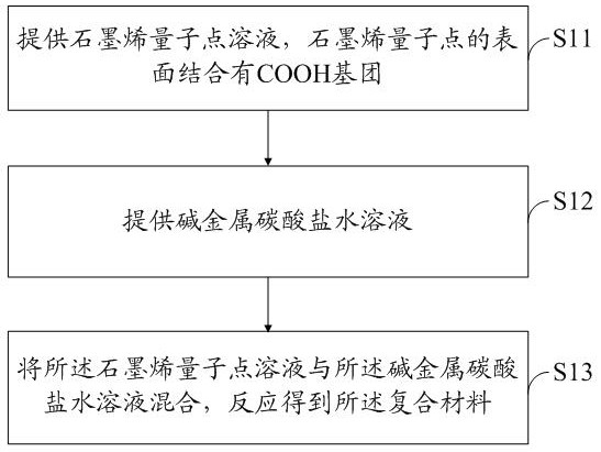
[0068] The preparation steps of the composite material are as follows:
[0069] 2.5g of carbon black was added to a mixture of 100ml of concentrated sulfuric acid and 50ml of concentrated nitric acid, heated and stirred for 24 hours;
[0070] After the solution is cooled, add deionized water to dilute, and adjust the acidity of the solution to PH=1;
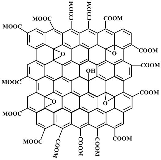
[0071] Adding excess acetone, removing the precipitate, and distilling the remaining solution to obtain a solid, which is the graphene quantum dot;
[0072] Dissolving the graphene quantum dot solid in an aqueous solvent with a concentration of 10mg / ml; and preparing an aqueous solution of alkali metal carbonate in advance with a concentration of 20mg / ml;
[0073] Gradually add an aqueous alkali metal carbonate solution to the graphene quantum dot solution until the pH value of the solution reaches 7.
[0074] The above solution is distilled to obtain a solid, which is a composite material.
Embodiment 2
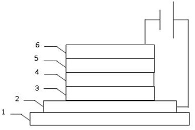
[0076] The preparation steps of the formal structure light-emitting diode are as follows:
[0077] Use transparent conductive film ITO as the anode, 50nm thick;
[0078] In the air environment, deposit PEDOT:PSS on the anode as a hole injection layer by solution method, with a thickness of 30nm, and anneal in air at 150°C for 10 minutes;
[0079] In a nitrogen environment, deposit TFB on the hole injection layer as a hole transport layer by solution method, with a thickness of 30nm, and anneal at 150°C for 30 minutes in a nitrogen environment;
[0080] In a nitrogen environment, deposit CdSe / ZnS as a quantum dot light-emitting layer on the hole transport layer by solution method, with a thickness of 25nm, and anneal at 80°C for 30 minutes in a nitrogen environment;
[0081] In a nitrogen environment, use a solution method to deposit graphene quantum dots bound to the surface of cesium on the quantum dot light-emitting layer as an electron transport layer, with a thickness of ...
Embodiment 3
[0084] The preparation steps of the trans-structure light-emitting diode are as follows:
[0085] Use transparent conductive film ITO as the cathode, 50nm thick;
[0086] In a nitrogen environment, use a solution method to deposit graphene quantum dots bound to the surface of cesium on the cathode as an electron transport layer, with a thickness of 40nm, and anneal at 70°C for 20 minutes in a nitrogen environment;
[0087] In a nitrogen environment, deposit CdSe / ZnS as a quantum dot light-emitting layer on the electron transport layer by solution method, with a thickness of 25nm, and anneal at 80°C for 30 minutes in a nitrogen environment;
[0088] Transfer the substrate to the evaporation chamber and vacuum to 10 -5 Pa level, TCTA is vapor deposited on the quantum dot light-emitting layer as a hole transport layer, with a thickness of 40nm;
[0089] Evaporate and deposit HAT-CN on the hole transport layer as a hole injection layer, 10nm thick;
[0090] Al was evaporated on...
PUM
 Abstract
Description
Claims
Application Information