Organic light-emitting display device and display device
An electroluminescent device and luminescent technology, applied in the direction of electric solid state devices, electrical components, semiconductor devices, etc., can solve the problems that can no longer meet the needs
- Summary
- Abstract
- Description
- Claims
- Application Information
AI Technical Summary
Problems solved by technology
Method used
Image
Examples
Synthetic example
[0068] Receptor molecule synthesis method:
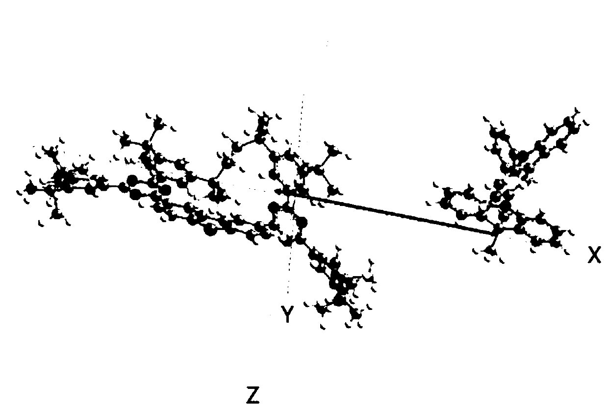
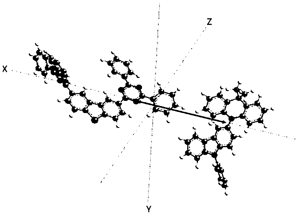
[0069] Under nitrogen protection, 3-bromo-9-phenylcarbazole (7.5mmol), 9,10-dihydroacridine (13.5mmol), tris(dibenzylideneacetone)-dipalladium (0.8mmol), A mixture of sodium tert-butoxide (35 mmol) and tri-tert-butylphosphine tetrafluoroborate (0.96 mmol) was placed in a three-necked flask filled with 200 mL of toluene and stirred at a temperature of 80-105° C. for 12 h. A mixture of ice and water was added to quench the reaction. After room temperature, the compound 1-17 was purified by vacuum filtration, followed by column chromatography and dried in vacuum. Yield: 85%.
[0070] The molecular weight obtained by mass spectrometry: 1050.69.
[0071] Receptor compound synthesis method:
[0072] Under nitrogen, 2-chloro-4,6-bis(3,5-di-tert-butylphenyl)-1,3,5-triazine (15 mmol), 2,8-diboronate diphenyl And furan (7.2mmol), Pd (pph3) 4 (0.2mmol), K 2 CO 3 Put into 100mL tetrahydrofuran THF and stir and reflux at 80°C overnight. A...
Embodiment 1
[0080] The preparation method of the organic electroluminescent device in this embodiment can be carried out according to the following steps:
[0081] ①In a vacuum of 1×10 -5 Under the condition of Pa, an indium tin oxide (ITO) thin film with a film thickness of 100 nm was deposited on a glass substrate as an anode 1 by a vacuum evaporation method.
[0082] ② Afterwards, compound A was vapor-deposited on the anode with a film thickness of 5 nm to form a hole injection layer (HIL) 2 .
[0083] ③ On the hole injection layer 2, the compound B was subsequently vapor-deposited to a film thickness of 160 nm to function as the first hole transport layer (HTL-1) 3 .
[0084] ④ On the first hole transport layer film, compound C was vapor-deposited to a film thickness of 10 nm to function as the second hole transport layer (HTL-2) 4 .
[0085] ⑤ Co-evaporating compound 1-20 of the present application, compound 2-17 of the present application, and compound D (guest material) on the se...
Embodiment 2
[0092] Except that when forming the light-emitting layer, the compound 2-18 of the present application was used instead of the compound 2-17 in the above-mentioned Example 1, and the organic electroluminescent device was fabricated by the same method as above.
PUM
 Abstract
Description
Claims
Application Information


