
Eureka
For R&D, Eureka makes reading and utilizing patents & technical documents easy.
Eureka AIR
Designed for self-driven R&D workflows. Generate viable solutions, solve complex R&D challenges, empower your innovation with AI.

Eureka Materials
Designed for material experts only. Revolutionize your material R&D, from search, analyze, to developing new materials.

TechResearch
Generate reliable direction feasibility study reports for your R&D in just a few steps.

TechSeek
Discover and master advanced knowledge NOW. Basics, ideas, possibilities, all at once.

TechMind
As an expert in R&D Theories, TechMind can generates customized viable solutions instantly.

TechRisk
Analyze your overall solution with one click, know your potential R&D risks in advance.

TechMonitor
Get weekly tech updates, stay abreast of the latest tech innovations and key insights.
Vertical heterogeneous p-n junction structure device and preparation method thereof
A heterogeneous device technology, applied in the field of vertical hetero p-n junction structure devices and their preparation, can solve the problems of high cost, extremely high equipment requirements, complicated processes, etc., and achieves low production cost, low equipment requirements, and high production efficiency. Effect
- Summary
- Abstract
- Description
- Claims
- Application Information
AI Technical Summary
Problems solved by technology
Method used
Image

Examples
Embodiment 1
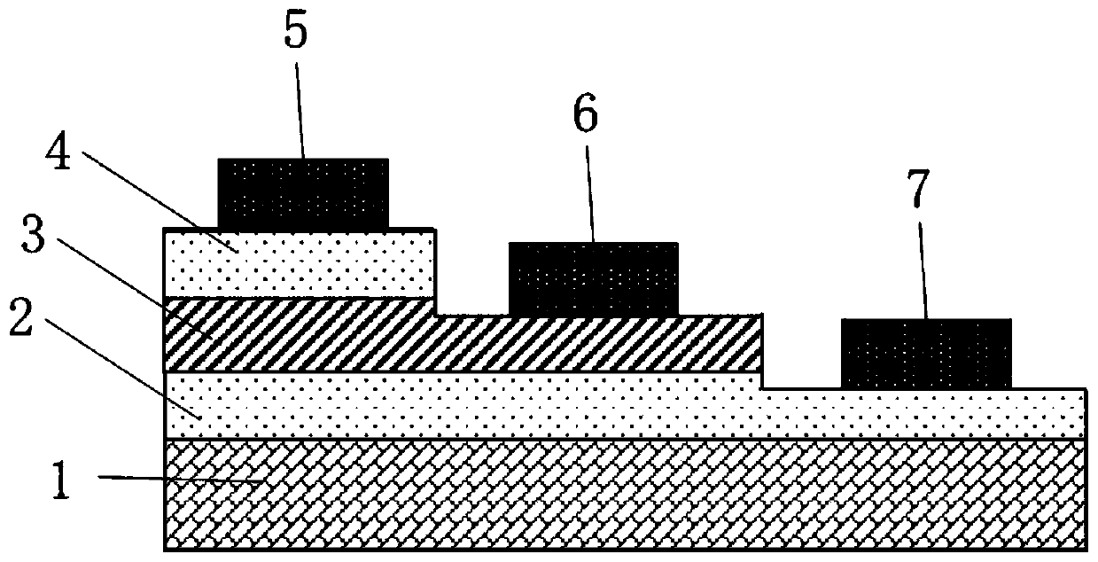
[0046]This embodiment provides a device with a vertical heterogeneous p-n junction structure and a preparation method thereof. The device includes: a sapphire substrate 1, a first n-type gallium nitride layer 2 located on the sapphire substrate 1, located in part of the n The p-type gallium oxide layer 3 above the p-type gallium oxide layer, the second n-type gallium nitride layer 4 above the part of the p-type gallium oxide layer, respectively located on the first n-type gallium nitride layer 2, p-type gallium nitride layer Type gallium oxide layer 3 and metal electrodes 7, 6, 5 on the second n-type gallium nitride layer 4. Such as figure 1 Shown is a schematic diagram of a device with a vertical heterogeneous p-n junction structure. Among them, the sapphire substrate 1 can also be a silicon substrate, a silicon carbide substrate, a diamond substrate, an aluminum nitride substrate, a gallium nitride homogeneous substrate, or a flexible substrate such as boron nitride, graphe...
Embodiment 2
[0055] This embodiment provides another annular p-n junction structure device and its preparation method, the device comprising: a sapphire substrate 1, a first n-type gallium nitride layer 2, located above the middle of the first n-type gallium nitride layer The p-type gallium oxide layer 3, the second n-type gallium nitride layer located above the p-type gallium oxide layer, and the metal electrode. Such as Figure 7 Shown is a schematic diagram of a circular p-n junction structure device.
[0056] The preparation method of the annular p-n junction structure device comprises:
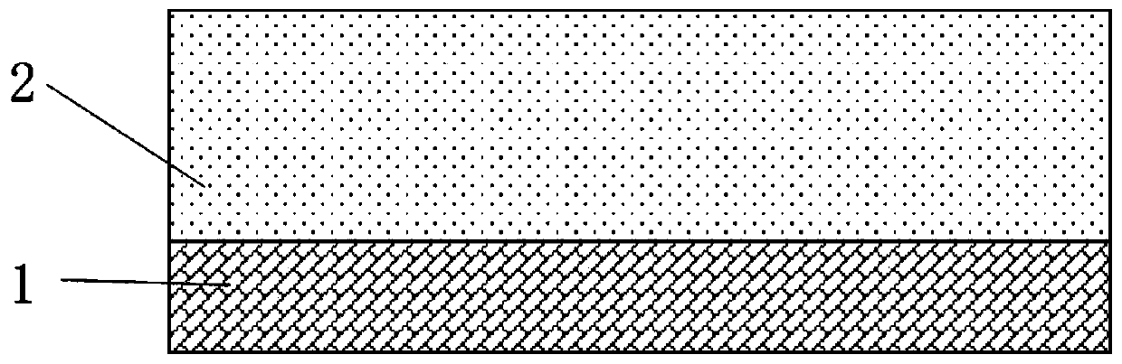
[0057] Step (1), growing a first n-type gallium nitride layer 2 on the sapphire substrate 1 with a thickness of 8 μm, figure 2 Schematic diagram of the grown GaN layer.
[0058] Step (2), covering the partially annular region on the grown first n-type gallium nitride layer 2 with a silicon dioxide mask layer 8 by atomic layer deposition, Figure 8 A schematic diagram of the covering mask layer. ...
Embodiment 3
[0064] This embodiment provides a diffusion growth carrier concentration of 1×10 in Step (3) of Embodiment 2. 11 ~1×10 20 / cm 3 The method for the p-type gallium oxide layer, the specific steps are as follows:
[0065] (1) Maintain the pressure in the chemical vapor deposition equipment cavity at 1.01×10 5 Pa, and continuously feed argon with a flow rate of 700 sccm as a reaction gas for 120 minutes.
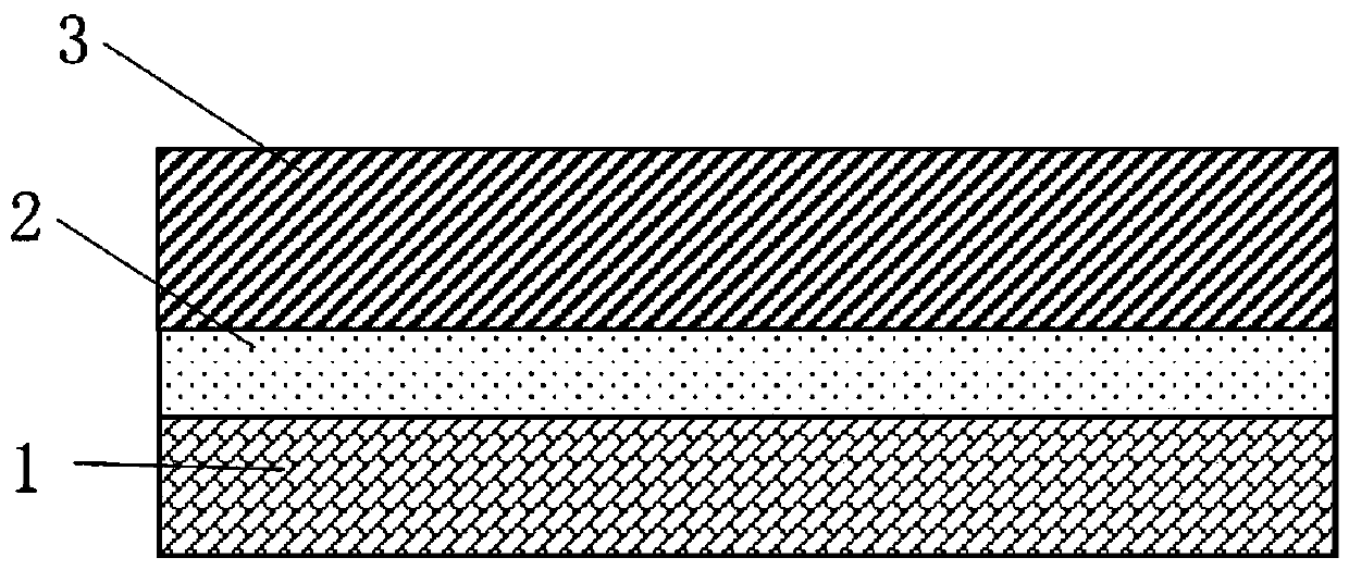
[0066] (2) Rapidly raise the temperature of the cavity to 1200°C, maintain 1200°C for 60 minutes for annealing, and diffusely grow a p-type gallium oxide film on the n-type gallium nitride layer 2 from the surface far away from the substrate to the surface close to the substrate.
PUM
| Property | Measurement | Unit |
|---|---|---|
| thickness | aaaaa | aaaaa |
| thickness | aaaaa | aaaaa |
| thickness | aaaaa | aaaaa |
Abstract
Description
Claims
Application Information
 - R&D Engineer
- R&D Manager
- IP Professional
- Industry Leading Data Capabilities
- Powerful AI technology
- Patent DNA Extraction
Browse by: Latest US Patents, China's latest patents, Technical Efficacy Thesaurus, Application Domain, Technology Topic, Popular Technical Reports.
© 2024 PatSnap. All rights reserved.Legal|Privacy policy|Modern Slavery Act Transparency Statement|Sitemap|About US| Contact US: help@patsnap.com