Eureka AIR delivers breakthrough ideas for toughest innovation challenges, trusted by R&D personnel around the world.

A kind of nitride level heterogeneous p-n junction structure device and its preparation method

A horizontal and heterogeneous technology, applied in semiconductor/solid-state device manufacturing, semiconductor devices, electrical components, etc., can solve the problems of high cost, low production efficiency, complex process, etc., to achieve low equipment requirements, low production cost, preparation Efficient effect

Active Publication Date: 2022-02-15
纳微朗科技(深圳)有限公司
View PDF6 Cites 0 Cited by
  • Summary
  • Abstract
  • Description
  • Claims
  • Application Information

AI Technical Summary

Problems solved by technology

However, there are many defects in the growth method, such as complex process, uneven p-n junction, and difficulty in doping control. Then form a p-n junction by recrystallization
The same alloy method also has disadvantages, such as the p-n junction is not smooth, the junction depth and the size of the junction are not easy to control, etc.; the ion implantation method refers to converting impurity atoms into ionized impurity ions first, and then injecting them in an extremely strong electric field Shoot the semiconductor at a high speed so that it can enter the interior of the semiconductor to achieve the purpose of doping
Although the ion implantation method overcomes the shortcomings of the first two methods, it has extremely high requirements for equipment, high cost, and low production efficiency; the diffusion method is currently the most commonly used method for manufacturing p-n junctions, which refers to the use of impurities at high temperature. Diffuse downward into the semiconductor, so that p-type impurities enter the n-type semiconductor or n-type impurities enter the p-type semiconductor to form a p-n junction
This method can not only precisely control the junction depth and junction area, but also maintain the flatness of the junction surface and doping concentration, but the high temperature introduced by the diffusion method when preparing the p-n junction may increase the lattice defects of the material

Method used


Image

  • A kind of nitride level heterogeneous p-n junction structure device and its preparation method
  • A kind of nitride level heterogeneous p-n junction structure device and its preparation method
  • A kind of nitride level heterogeneous p-n junction structure device and its preparation method

Examples


Embodiment 1

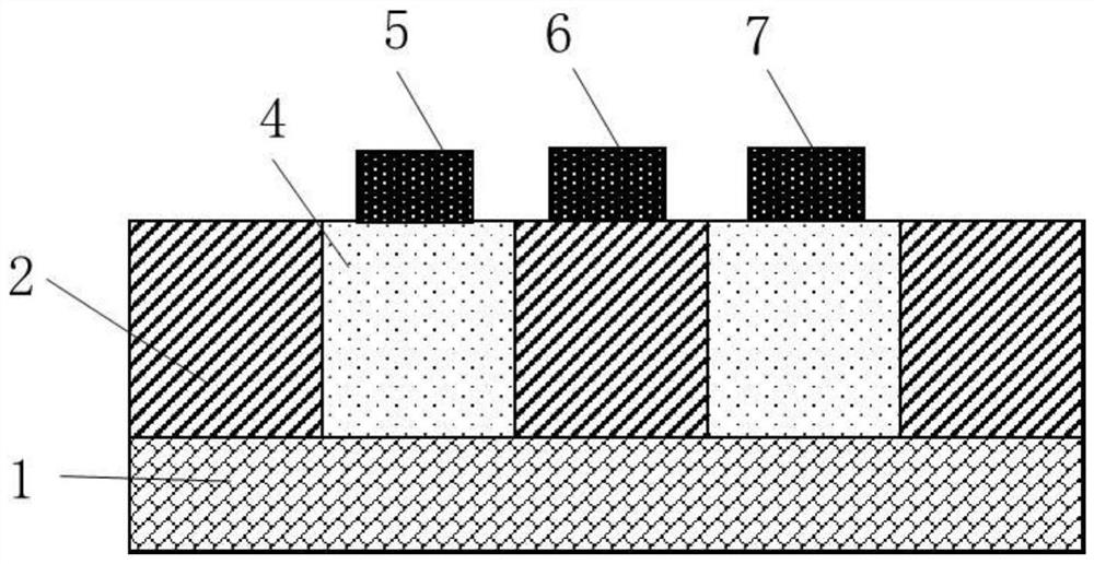
[0044] This embodiment provides a nitride level heterogeneous p-n junction structure device, the p-n junction structure device includes: a sapphire substrate, a p-type gallium oxide layer, an n-type gallium nitride layer embedded in the p-type gallium oxide layer, metal electrodes. Such as figure 1 Shown is a schematic diagram of a nitrided horizontal heterogeneous p-n junction structure device. The bottom layer is a sapphire substrate 1, and the substrate 1 can also be a silicon substrate, a silicon carbide substrate, a diamond substrate, an aluminum nitride substrate, a gallium nitride homogeneous substrate, or boron nitride, graphene, Flexible substrates such as copper nickel. On the substrate 1 are alternately arranged p-type gallium oxide layers 2 and n-type gallium nitride layers 4 . The carrier concentration of the n-type gallium nitride layer 4 is 1×10 11 ~1×10 19 / cm 3. The p-type gallium oxide layer can also be replaced by p-type indium oxide layer, p-type al...

Embodiment 2

[0046] This embodiment provides the preparation method of the nitride level heterogeneous p-n junction structure device in the first embodiment. It mainly includes the following steps:

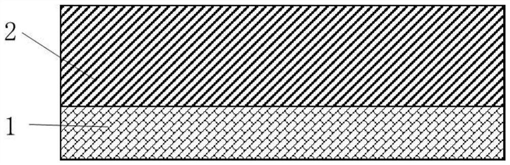
[0047] Step (1), growing a p-type gallium oxide layer 2 on the sapphire substrate 1 with a thickness of 3 μm, figure 2 It is a schematic diagram of the grown p-type gallium oxide layer.

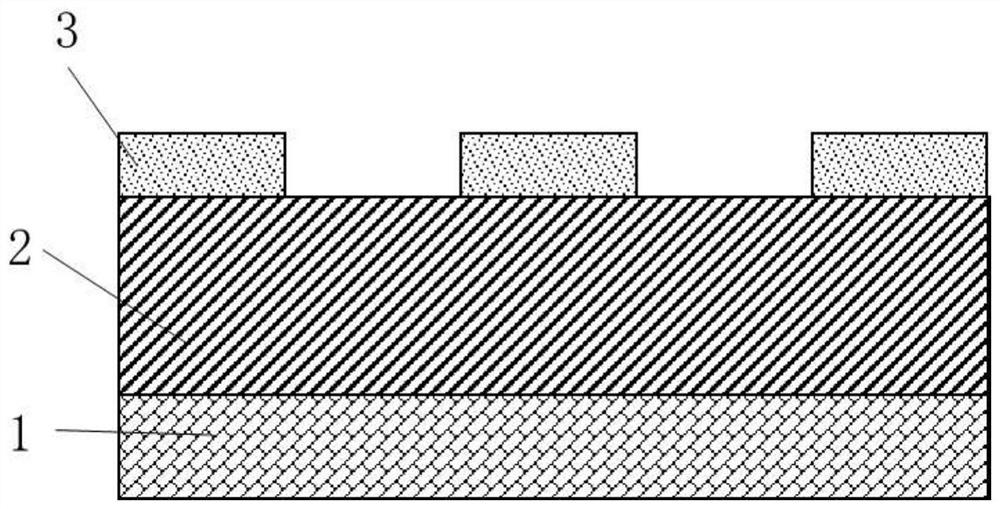
[0048] In step (2), on the p-type gallium oxide layer 2, a layer of silicon nitride mask 3 with a certain pattern is deposited on the p-type gallium oxide layer 2 by atomic vapor deposition, image 3 It is a schematic diagram after depositing a mask layer on the p-type gallium nitride layer.

[0049] In step (3), by chemical vapor deposition, on the region of the p-type gallium oxide layer 2 not covered with the mask 3, the carrier concentration is 1×10 by thermal nitriding diffusion from the upper surface to the lower surface 11 ~1×10 20 / cm 3 n-type gallium nitride layer 4, so that the n-type gallium ...

Embodiment 3

[0054] This embodiment provides a heterojunction field effect transistor device based on a horizontal heterogeneous p-n junction structure and its preparation method. The heterojunction field effect transistor device includes: a sapphire substrate 1, a p-type gallium oxide layer 2, an embedded The n-type gallium nitride layer 4 inside the p-type gallium oxide layer 2 and the metal electrodes 5, 6, 7. Such as Figure 6 Shown is a schematic diagram of a heterogeneous p-n junction field effect transistor device.

[0055] The preparation method of the heterojunction field effect transistor device includes:

[0056] Step (1), growing a p-type gallium oxide layer 2 on the sapphire substrate 1 with a thickness of 3 μm, figure 2 Schematic diagram of the grown gallium oxide layer.

[0057] Step (2), on the p-type gallium oxide layer 2, deposit a layer of hafnium dioxide on the p-type gallium oxide layer as a mask 3 by means of atomic vapor deposition, Figure 7 It is a schematic d...


PUM

PropertyMeasurementUnit
thicknessaaaaaaaaaa
thicknessaaaaaaaaaa

Abstract

The invention discloses a nitriding level heterogeneous p-n junction structure device and a preparation method thereof, and belongs to the field of semiconductor devices. The nitrided level heterogeneous p-n junction structure device comprises: a substrate, a p-type material layer, An n-type material layer embedded inside the p-type material layer, and a metal electrode on the upper surface of the p-type material layer and the n-type material layer. Among them, the selective growth of the n-type material layer is realized by covering the p-type material layer with a mask layer with a specific pattern, and a horizontal heterogeneous p-n junction structure can be obtained after the growth is completed. The invention has a simple process and is expected to expand the application of oxide semiconductor materials such as gallium oxide and indium oxide.

Description

technical field [0001] The invention belongs to the field of semiconductors, in particular to a nitride level heterogeneous p-n junction structure device and a preparation method thereof. Background technique [0002] With the rapid development of the semiconductor industry, the oxide semiconductor p-n junction has become a research hotspot. Due to the intrinsic defects of oxides and the limitation of preparation technology, stable and high-performance p-type hole-conducting materials are scarce. For most oxide crystals, the n-type semiconductor is easy to form, and the control of the carrier concentration in a large range has been realized through the doping of atoms such as Si and Sn. [0003] In recent studies, p-type oxide materials have become a research hotspot, and many high-quality p-type materials have been preliminarily prepared. As one of the important applications of p-type materials, the p-n junction occupies a very important position in the field of electroni...

Claims


Application Information

Patent Timeline
Patent Type & Authority Patents(China)
IPC IPC(8): H01L29/06H01L29/78H01L21/336H01L21/02
CPCH01L29/78H01L29/0684H01L29/66446H01L21/0254H01L21/02636
Inventor 方志来闫春辉蒋卓汛吴征远田朋飞张国旗
Owner 纳微朗科技(深圳)有限公司
Why Eureka
Eureka Blog
Learn More