Design method of integrated photonic band-pass filter based on genetic optimization

A band-pass filter and genetic optimization technology, applied in the fields of genetic law, waveguide devices, design optimization/simulation, etc., can solve the problems of complicated design process and large volume, and achieve improved design efficiency, large bandwidth and good performance. Effect

Active Publication Date: 2020-07-17
BEIJING INSTITUTE OF TECHNOLOGYGY
View PDF6 Cites 0 Cited by
  • Summary
  • Abstract
  • Description
  • Claims
  • Application Information

AI Technical Summary

Problems solved by technology

[0004] The purpose of the present invention is to provide a method for designing an integrated photonic band-pass filter based on genetic op

Method used


Image

  • Design method of integrated photonic band-pass filter based on genetic optimization
  • Design method of integrated photonic band-pass filter based on genetic optimization
  • Design method of integrated photonic band-pass filter based on genetic optimization

Examples


Embodiment 1

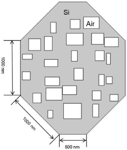
[0032] This embodiment describes the design method of the integrated photonic bandpass filter based on genetic optimization according to the present invention. The octagon with the upper and lower bases of 500nm and the remaining sides of 1000nm is used as the overall structure of the device, and the rectangle is used as the structural unit. Design a bandpass filter.

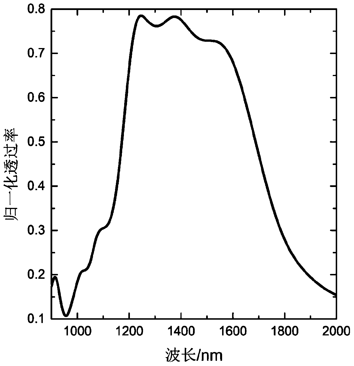
[0033] Use a 6×5 equidistant grid to divide the octagon, and choose silicon and air as materials. The light in the 900-1800nm ​​band enters from the center of the left end, and the light in the 1200-1650nm band exits from the center of the right end.

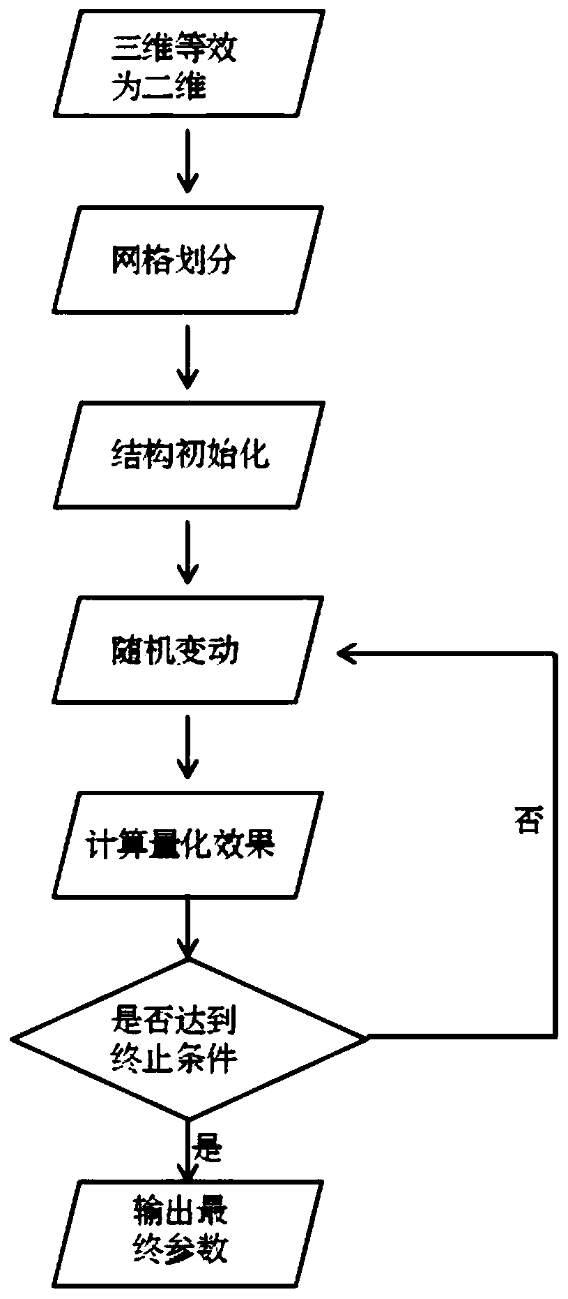
[0034] The equivalent refractive index of the system at the central wavelength position is obtained by using the mode analysis module of the physical field simulation software, and the two-dimensional model is used instead of the three-dimensional model to achieve the purpose of reducing the amount of calculation. The equivalent refractive index method can take i...


PUM


Abstract

The invention relates to a design method of an integrated photonic band-pass filter based on genetic optimization, and belongs to the technical field of micro-nano photonics devices. A mode analysis module of physical field simulation software is utilized, an equivalent refractive index method is adopted to enable a three-dimensional model to be equivalent to a two-dimensional model, the overall shape and the structural unit shape of a device are selected, and then an equidistant grid is used for dividing the overall device to carry out genetic optimization operation, so that the structure ofthe band-pass filter is determined through an output optimal structural unit. According to the method, the design efficiency is greatly improved, and compared with a traditional macroscopic optical device, the manufactured band-pass filter is ultra-small in size and high in integration degree, has good performances and excellent linear type, is large in bandwidth and is low in roll-off range; andthe indexes meet the requirements of current micro-nano machining. By using the method, a researcher can focus on cascade application of the device and exploration of an internal mechanism of the device, and an alternative scheme is provided for development of optical processing and optical communication in the future.

Description

technical field [0001] The invention relates to a design method of an integrated photonic bandpass filter based on genetic optimization, and belongs to the technical field of micro-nano photonic devices. Background technique [0002] With the rise of new industries including 5G communications and the Internet of Things, the demand for high-speed, low-loss information processing systems in practical applications is increasing day by day. Limited by Moore's Law, traditional electronic devices face bottlenecks in breakthroughs in storage density and computing speed, and entering the "post-Moore era", electronic devices cannot be integrated without limit. The smaller the size of the device, the more obvious the quantum effect, and the greater the difficulty of integration. As a continuation of Moore's Law, people have proposed a design with great potential - photonic chip. Compared with traditional electronic chips, one of the great advantages of photonic chips is that there i...

Claims


Application Information

Patent Timeline
IPC IPC(8): G06F30/20G06N3/12H01P11/00
CPCG06N3/126H01P11/00H01P11/007
Inventor 路翠翠袁弘毅马丽凤王慧琴刘舟慧
Owner BEIJING INSTITUTE OF TECHNOLOGYGY
Why Eureka
Try Eureka