Preparation method of dielectric film with ultrahigh dielectric constant

A technology of dielectric film and dielectric constant, which is applied in the manufacture of circuits, electrical components, semiconductors/solid-state devices, etc., can solve problems such as not being able to meet process requirements, achieve low equivalent gate oxide thickness, ultra-high dielectric constant, reduce Lattice Distortion Effects

Active Publication Date: 2020-07-17
SHANGHAI NORMAL UNIVERSITY
View PDF4 Cites 3 Cited by
  • Summary
  • Abstract
  • Description
  • Claims
  • Application Information

AI Technical Summary

Problems solved by technology

The dielectric constant of the high-k dielectric prepared by this method is 10-25, which cannot meet the process requirements of 10nm and later technology nodes

Method used


Image

  • Preparation method of dielectric film with ultrahigh dielectric constant
  • Preparation method of dielectric film with ultrahigh dielectric constant
  • Preparation method of dielectric film with ultrahigh dielectric constant

Examples


Embodiment Construction

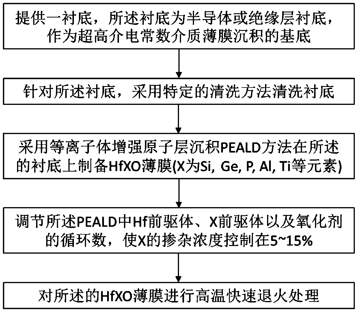
[0027] The specific implementation of a method for preparing an ultra-high dielectric constant dielectric film provided by the present invention will be described in detail below in conjunction with the accompanying drawings. figure 1 Its main steps are as follows:

[0028] Select a substrate, and here we choose the most common Si wafer substrate as an example. In this example, first use NH with a volume ratio of 1:1:5 3 ·H 2 O, H 2 o 2 、H 2O mixed solution to clean the Si substrate, the cleaning time is 10min, and then use the volume ratio of 1% HF aqueous solution to clean the Si substrate, the cleaning time is 30s; finally use the volume ratio of 1:1:6 HCl, h 2 o 2 、H 2 O solution was used to clean the Si substrate, and the cleaning time was 10 min.

[0029] The cleaned substrate is further placed in the reaction chamber of plasma enhanced atomic layer deposition PEALD, and a nanometer-thick HfXO film is deposited on the surface of the substrate (X is Si, Ge, P, Al...


PUM

PropertyMeasurementUnit
pore sizeaaaaaaaaaa

Abstract

The invention discloses a preparation method of a dielectric film with an ultrahigh dielectric constant. The method comprises the following steps: (1) providing a substrate and cleaning the substrateto serve as a substrate for depositing the dielectric film; (2) preparing an HfXO thin film on the substrate by adopting a plasma enhanced atomic layer deposition method, wherein X is Si, Ge, P, Al orTi, and the number of atoms of X doped in HfXO accounts for 5-15%; and (3) carrying out high-temperature rapid annealing treatment on the HfXO film. By forming a crystalline phase structure with an ultrahigh dielectric constant, the preparation of the dielectric film with the ultrahigh dielectric constant is realized. According to the preparation method, the dielectric film with low equivalent gate-oxide thickness, ultrahigh dielectric constant, wide energy gap and high reliability can be prepared, and a feasible path is provided for selection of gate-oxide media in a semiconductor process technology which is rapidly developed along with the Moore law at present.

Description

technical field [0001] The invention belongs to the technical field of microelectronics and solid electronics, and in particular relates to a preparation method of an ultra-high dielectric constant dielectric thin film. Background technique [0002] The improvement of semiconductor integration requires the continuous reduction of the feature size of microelectronic devices, and the traditional semiconductor channel materials and dielectric insulating materials are facing physical limits. In addition, with the advent of the era of cloud computing, big data, and green energy, the demand for high-speed, high-power-density, and higher-energy-efficiency power conversion systems is increasing day by day. Whether the development of semiconductor technology continues Moore's Law or surpasses Moore's Law, research on new materials, new devices, and new processes is indispensable. [0003] For a MOSFET device, its drive current is a very important influencing parameter, which determi...

Claims


Application Information

Patent Timeline
Patent Type & Authority Applications(China)
IPC IPC(8): H01L21/28H01L21/285C23C16/40C23C16/50C23C16/56
CPCH01L21/285H01L21/28158C23C16/405C23C16/40C23C16/50C23C16/56
Inventor 曹铎刘锋林方婷张毅闻何晓勇石旺舟
Owner SHANGHAI NORMAL UNIVERSITY
Why Eureka
Try Eureka