Solid-state imaging device, method for driving solid-state imaging device, and electronic apparatus

A camera device, solid-state technology, applied in TV, electrical components, color TV, etc., can solve the problem of unable to read the global shutter, and achieve the effect of large dynamic range, noise reduction, and expansion of effective pixel area

Active Publication Date: 2020-07-21
普里露尼库斯新加坡私人有限公司
View PDF12 Cites 1 Cited by
  • Summary
  • Abstract
  • Description
  • Claims
  • Application Information

AI Technical Summary

Problems solved by technology

[0008] However, although this type of CMOS image sensor can transmit signals at high speed, it has the disadvantage that global shutter reading cannot be performed.

Method used


Image

  • Solid-state imaging device, method for driving solid-state imaging device, and electronic apparatus
  • Solid-state imaging device, method for driving solid-state imaging device, and electronic apparatus
  • Solid-state imaging device, method for driving solid-state imaging device, and electronic apparatus

Examples


no. 1 approach

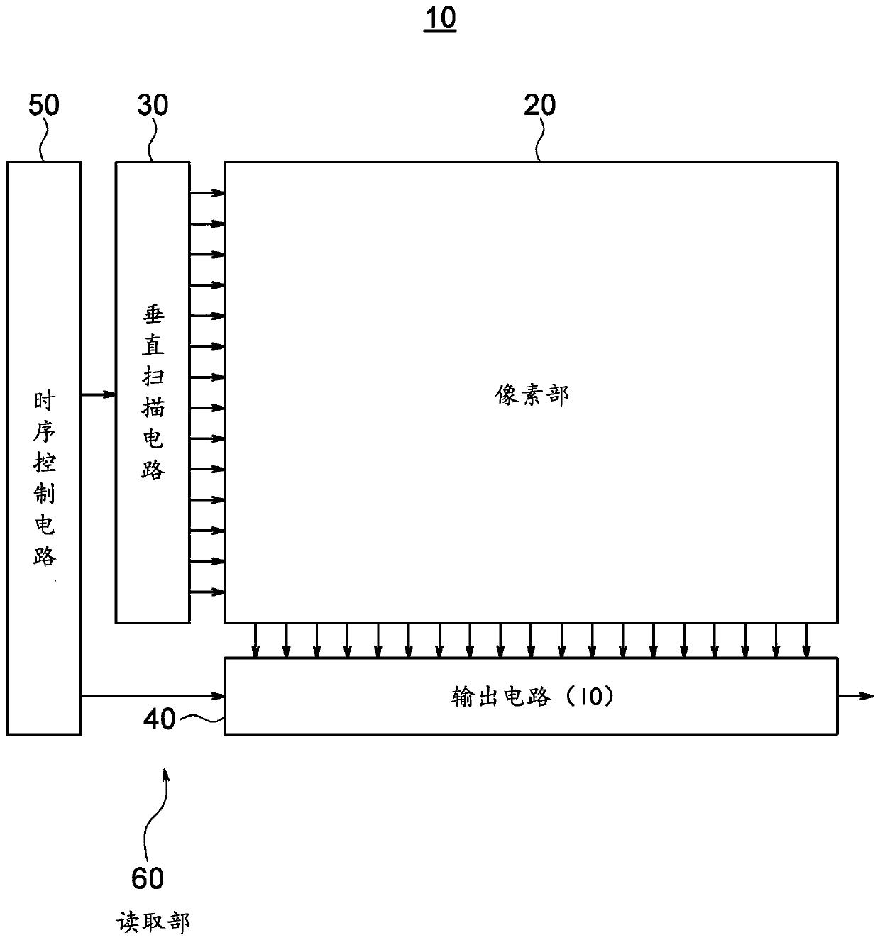
[0067] figure 1 It is a block diagram showing a configuration example of the solid-state imaging device according to the first embodiment of the present invention.

[0068] In the present embodiment, the solid-state imaging device 10 is constituted by, for example, a CMOS image sensor including digital pixels (Digital Pixels) as pixels.

[0069] Such as figure 1 As shown, this solid-state imaging device 10 includes a pixel unit 20 as an imaging unit, a vertical scanning circuit (row scanning circuit) 30, an output circuit 40, and a timing control circuit 50 as main constituent elements.

[0070] Among these components, for example, the vertical scanning circuit 30, the output circuit 40, and the timing control circuit 50 constitute a pixel signal reading unit 60.

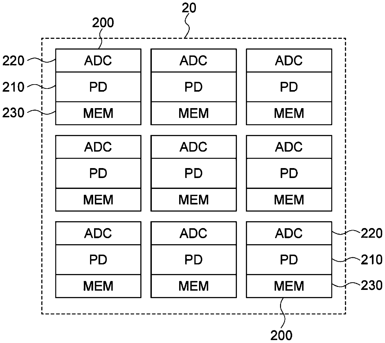
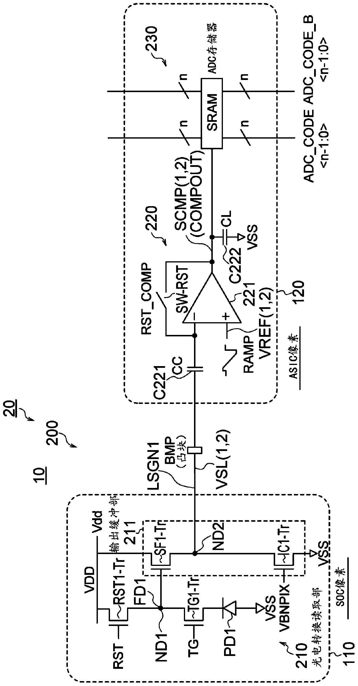
[0071] In the first embodiment, the solid-state imaging device 10 includes, as digital pixels, a photoelectric conversion reading unit, an AD (analog-to-digital) conversion unit, and a memory unit in the pixel uni...

no. 2 approach

[0330] Figure 17 It is a circuit diagram showing a configuration example of a comparator according to the second embodiment.

[0331] The difference between the solid-state imaging device 10A of the second embodiment and the solid-state imaging device 10 of the first embodiment is as follows.

[0332] In the solid-state imaging device 10A of the second embodiment, the second noise band limiting capacitor C752 is connected to the input line of the voltage signal VSL to the auto-zero capacitor C711 of the first amplifier 710 from the pixel output buffer unit 211.

[0333] The source follower output of a pixel includes a typical parasitic capacitance of 1 to 2 pF that functions as a noise bandwidth limiting capacitor, but the source follower output of a DPS pixel is different from a typical rolling shutter CMOS image sensor that does not have these parasitic capacitances. different. Therefore, the higher frequency noise spectrum is transferred to the comparator, which overall ...

no. 3 approach

[0337] Figure 18 It is a circuit diagram showing a configuration example of a comparator according to the third embodiment.

[0338] The difference between the solid-state imaging device 10B of the third embodiment and the solid-state imaging device 10A of the second embodiment is as follows.

[0339] In the solid-state imaging device 10B of the third embodiment, the gate of the other NMOS transistor NT713 of the differential transistor pair DTP is connected to the third noise band limiting capacitor C753.

[0340] In the comparator 700B of the third embodiment, in order to suppress the AZ switching transistor noise during the AZ period, the parasitic capacitance of the third noise bandwidth limiting capacitor C753 connected to the node ND713 is small, so high voltage noise appears.

[0341] Therefore, adding the third noise bandwidth limiting capacitor C753 (CL3) will effectively reduce the AZ noise.


PUM


Abstract

Provided are a solid-state imaging device, a method for driving the same and an electronic apparatus where a comparator in an AD converter in a digital pixel is characterized by low power consumptionand low peak current and that are capable of operating at low voltage and achieving high linearity across the entire input range. A comparator 700 is constituted by two stages of preamplifiers 710 and720 with a clamp diode and two serial current-controlling inverters 730 and 740, and every branch is current-controlled. The two stages of the preamplifiers 710 and 720 and the following two consecutive inverters 730 and 740 are all current-controlled such that low power consumption and low peak current are realized. A trade-off can be made between the noise and the comparator speed by controlling the bandwidth of the comparator using the bias current. This is beneficial to more than one comparator operation mode.

Description

technical field [0001] The present invention relates to a solid-state imaging device, a driving method of the solid-state imaging device, and electronic equipment. Background technique [0002] A Complementary Metal Oxide Semiconductor (CMOS) image sensor has been put into practical use as a solid-state imaging device (image sensor) using a photoelectric conversion element that detects light and generates charges. [0003] CMOS image sensors are widely used as part of various electronic devices such as digital cameras, video cameras, surveillance cameras, medical endoscopes, personal computers (PCs), mobile phones and other portable terminal devices (mobile devices). [0004] The CMOS image sensor has an FD amplifier including a photodiode (photoelectric conversion element) and a floating diffusion layer (FD: Floating Diffusion, floating diffusion layer) in each pixel. The mainstream reading type of the CMOS image sensor is column-parallel output type, that is, select a cer...

Claims


Application Information

Patent Timeline
Patent Type & Authority Applications(China)
IPC IPC(8): H04N5/374H04N5/357
CPCH04N25/60H04N25/76H04N25/57H04N25/772H04N25/79H04N25/75H04N25/65
Inventor 大高俊德
Owner 普里露尼库斯新加坡私人有限公司
Why Eureka
Try Eureka