A design method of bgo crystal used in optical waveguide field sensor

A BGO crystal and design method technology, applied in chemical instruments and methods, crystal growth, electrostatic field measurement, etc., can solve the problems of increasing sensor volume and manufacturing cost, reducing measurement accuracy, measurement error, etc., to achieve good optical performance, melting point Low, avoids the effect of experimental error

Active Publication Date: 2021-07-20
CHINA UNIV OF GEOSCIENCES (WUHAN) +1
View PDF4 Cites 0 Cited by
  • Summary
  • Abstract
  • Description
  • Claims
  • Application Information

AI Technical Summary

Problems solved by technology

On the one hand, this kind of scheme uses a variety of optical devices, and the coupling between these optical devices will inevitably produce cumulative errors, and increase the volume and production cost of the sensor; on the other hand, the light inside the crystal is not affected by the crystal light. The guidance of the waveguide is easy to cause the problem of light divergence, resulting in the reduction of measurement accuracy
[0007] The optical electric field sensor has been extensively studied because of its good performance, but due to the influence of its structural design and manufacturing process, it will cause a certain degree of measurement error

Method used


Image

  • A design method of bgo crystal used in optical waveguide field sensor
  • A design method of bgo crystal used in optical waveguide field sensor
  • A design method of bgo crystal used in optical waveguide field sensor

Examples


Embodiment Construction

[0033] The technical solution will be clearly and completely described below in conjunction with the embodiments of the present invention. Apparently, the described embodiments are only some of the embodiments of the present invention, not all of them. Based on the embodiments of the present invention, all other embodiments obtained by persons of ordinary skill in the art without making creative efforts belong to the protection scope of the present invention.

[0034] The technical solution adopted in the embodiment of the present invention is: a method for designing a BGO crystal used in an optical waveguide field sensor, comprising the following steps:

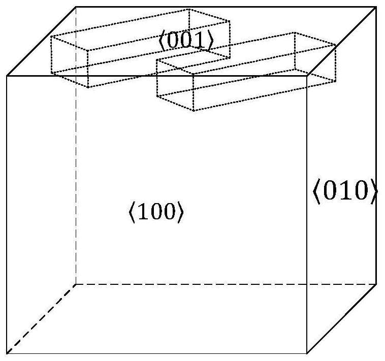
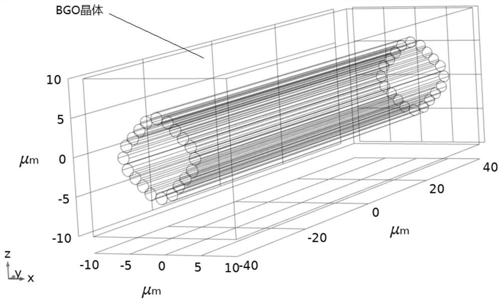
[0035] S1: the raw material Bi 2 o 3 and GeO 2 Put in a crucible and heat to melt to get Bi 2 o 3 and GeO 2 Then the seed crystal is immersed in the melt, while the melt is pulled and rotated to induce crystallization of the melt to obtain BGO cubic crystals. During the crystallization process of BGO cubic crystals, di...


PUM

PropertyMeasurementUnit
diameteraaaaaaaaaa
heightaaaaaaaaaa
radiusaaaaaaaaaa

Abstract

The invention discloses a method for designing a BGO crystal used in an optical waveguide field sensor. Firstly, the raw material Bi 2 o 3 and GeO 2 Prepare BGO cubic crystals, cut BGO cubic crystals to obtain BGO crystals of standard size, then use femtosecond laser to carve two symmetrical optical waveguides inside the BGO crystal, and use laser to carve parallel grooves on both sides of one of the optical waveguides , and use the method of electron beam spraying to make Au metal electrodes in the groove, and finally use the active alignment technology to adjust the relative position of the components by detecting the coupled optical power, and use the refractive index matching type curing glue between the optical fiber and the crystal end face. Match and fix. The BGO crystal provided by the invention has high purity and high transmittance, which greatly reduces the measurement error caused by the quality problem of the electro-optic crystal itself.

Description

technical field [0001] The invention belongs to the field of BGO crystal cutting and processing, and in particular relates to a design method of a BGO crystal used in an optical waveguide field sensor. Background technique [0002] Optical electric field sensors have attracted more and more attention in the field of electric field measurement. Compared with traditional active electric field sensors, they have the advantages of small size, high precision, high sensitivity, large linear dynamic range, and wide frequency response. Optical electric field sensors It has broad application prospects and research value. Existing optical electric field sensors are mostly composed of a crystal optical path and an output light detection circuit. For the crystal optical path, the existing preparation methods will affect the optical characteristics of the electro-optic crystal, so as to reduce the measurement accuracy of the entire electric field sensor. [0003] BGO crystal has good el...

Claims


Application Information

Patent Timeline
Patent Type & Authority Patents(China)
IPC IPC(8): C30B15/00C30B28/10C30B29/32C23C14/30C23C14/18G01R29/12G16C60/00
CPCC23C14/18C23C14/30C30B15/00C30B28/10C30B29/32G01R29/12G16C60/00
Inventor 王瑾胡煌季启政冯娜陈秋荻龙丹
Owner CHINA UNIV OF GEOSCIENCES (WUHAN)
Why Eureka
Try Eureka