Manufacturing method of film with controllable thermal conductivity and micro-nano structure

A technology of micro-nano structure and manufacturing method, which is applied in the fields of thin film manufacturing and micro-nano processing, can solve the problems of reducing and flexibly regulating the increase of thermal conductivity, and achieves the effect of high controllability and high success rate

Inactive Publication Date: 2020-08-04
BEIJING INSTITUTE OF TECHNOLOGYGY
View PDF11 Cites 0 Cited by
  • Summary
  • Abstract
  • Description
  • Claims
  • Application Information

AI Technical Summary

Problems solved by technology

[0005] Although the above-mentioned methods can control the thermal conductivity of the thin film, their methods are highly targeted, mainly for a certain type of specific material, and are not suitable for other materials.
Moreover, many methods can only achieve one-way regulation of thermal conductivity, and it is difficult to flexibly control the increase and decrease of thermal conductivity.

Method used


Image

  • Manufacturing method of film with controllable thermal conductivity and micro-nano structure
  • Manufacturing method of film with controllable thermal conductivity and micro-nano structure
  • Manufacturing method of film with controllable thermal conductivity and micro-nano structure

Examples


Embodiment 1

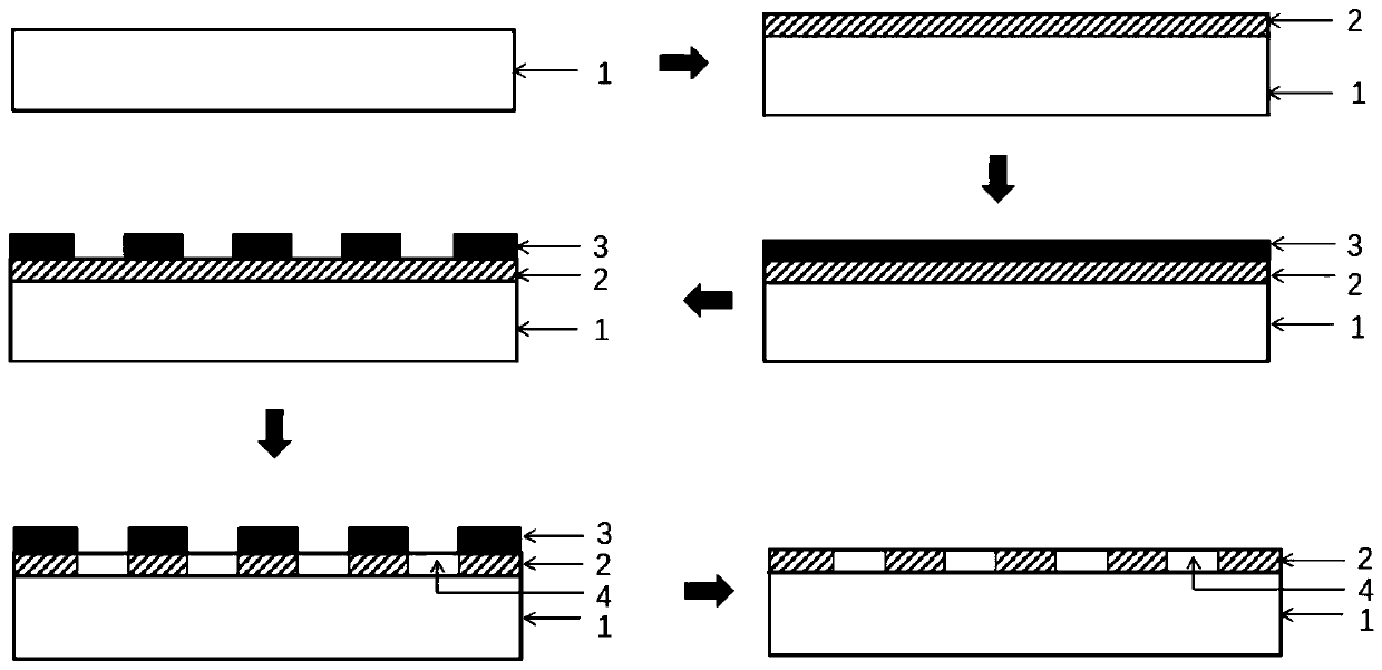
[0031] Embodiment 1: Taking the preparation of polyimide (PI) solid film as an example, adopt the preparation method of the present invention to reduce the thermal conductivity of PI solid film 2, and its technological process is as follows figure 1 As shown, the specific production method is as follows:

[0032] Step 1: Select (100) crystal-oriented N-type single-sided polished circular silicon wafer 1 as the substrate, the thickness of the silicon wafer 1 is 500 μm, the diameter is 4 inches, and the polished surface is used as the operation surface. Clean the substrate operation surface: use acetone, alcohol, and deionized water to ultrasonically clean the substrate for 10 minutes in sequence, and use nitrogen to dry the operation surface after cleaning.

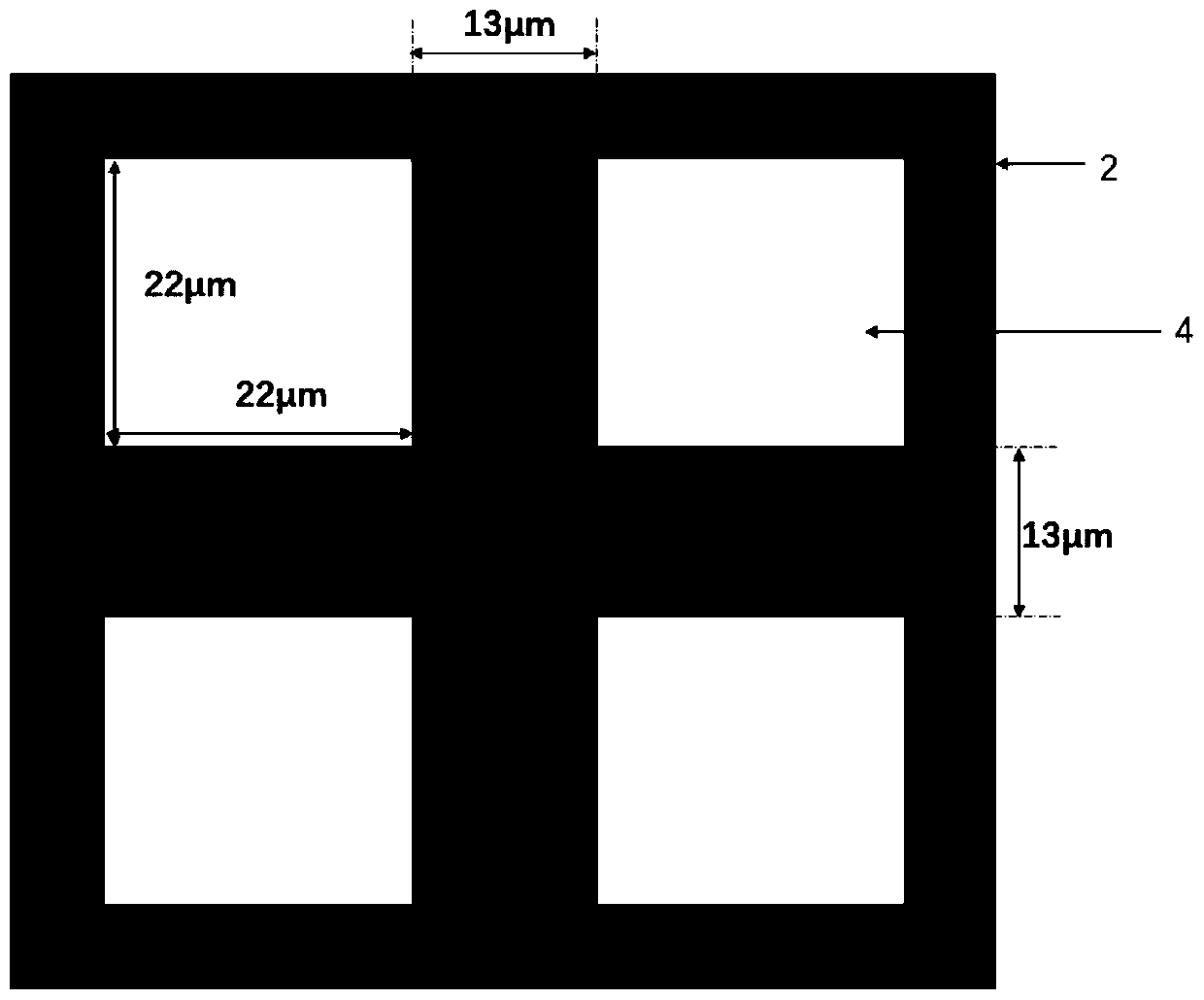
[0033] Step 2: Prepare a circular PI solid film 2 with a diameter of 4 inches and a thickness of 0.5 μm on the operating surface of the silicon wafer 1 by using a homogenizer. Solid content of PI solution: 12%, viscosity ...

Embodiment 2

[0038] Embodiment 2: the comparative example of embodiment 1

[0039] Step 1: Select (100) crystal-oriented N-type single-sided polished circular silicon wafer 1 as the substrate, the thickness of the silicon wafer 1 is 500 μm, the diameter is 4 inches, and the polished surface is used as the operation surface. Clean the substrate operation surface: use acetone, alcohol, and deionized water to ultrasonically clean the substrate for 10 minutes in sequence, and use nitrogen to dry the operation surface after cleaning.

[0040] Step 2: Prepare a circular PI solid film 2 with a diameter of 4 inches and a thickness of 0.5 μm on the operating surface of the silicon wafer 1 by using a homogenizer. Solid content of PI solution: 12%, viscosity 300-400cp; speed of homogenizer: pre-spin coating 800r / min, homogenization time 60s; fast spin coating 4000r / min, homogenization time 180s. After the spin coating, the PI solid film 2 is heat-treated, and the specific parameters are: bake at 100...

Embodiment 3

[0041] Embodiment 3: Taking the preparation of a silicon oxide solid film as an example, the preparation method of the present invention is used to improve the thermal conductivity of the silicon oxide solid film, and its process flow is as follows Figure 4 As shown, the specific production method is as follows:

[0042] Step 1: Select (100) crystal-oriented N-type single-sided polished circular silicon wafer 1 as the substrate, the thickness of the silicon wafer 1 is 500 μm, the diameter is 4 inches, and the polished surface is used as the operation surface. Clean the substrate operation surface: use acetone, alcohol, and deionized water to ultrasonically clean the substrate for 10 minutes in sequence, and use nitrogen to dry the operation surface after cleaning.

[0043] Step 2: Use the magnetron sputtering process to sputter a circular silicon oxide solid film 5 with a diameter of 4 inches and a thickness of 300 nm on the surface of the silicon wafer 1, with a sputtering r...


PUM

PropertyMeasurementUnit
thicknessaaaaaaaaaa
thicknessaaaaaaaaaa
thicknessaaaaaaaaaa

Abstract

The invention discloses a method for manufacturing a film with controllable thermal conductivity and a micro-nano structure. The method comprises the following steps: firstly, preparing a layer of solid film on a substrate; then processing a thermophysical property regulation and control region on the surface of the solid film; finally, filling the thermophysical property regulation and control area of the solid film with a thermophysical property regulation and control material, wherein the thermophysical property regulation and control area is one or more defect units distributed on the surface of the solid film according to the thermophysical property regulation and control requirement, the thermophysical property regulation and control material comprises a conductivity increasing material for improving the thermal conductivity of the solid film and a conductivity reducing material for reducing the thermal conductivity of the solid film, the conductivity increasing material is a solid material of which the thermal conductivity is higher than that of the solid film, and the conductivity reducing material is a solid material of which the thermal conductivity is lower than that ofthe solid film. According to the method for manufacturing the film, the heat conductivity of the solid thin film can be regulated and controlled.

Description

technical field [0001] The invention relates to a method for manufacturing a film with a micro-nano structure with controllable thermal conductivity, and belongs to the fields of film manufacturing and micro-nano processing. Background technique [0002] With the rapid development of microelectronics technology, the integration of chips is getting higher and higher. At the same time, the power density of microelectronic chips is also increasing. Some chips even have a surface power density of 100W / cm 2 . On a tiny chip, if the heat cannot be dissipated in time, the performance and reliability of the chip will be greatly affected. In addition to dissipating the heat on the chip surface, sometimes it is necessary to control the heat exchange rate on the chip surface to ensure the stability of the chip operation. Therefore, it is very important to control the heat exchange rate between the chip and the environment during the chip design and manufacturing process. [0003] S...

Claims


Application Information

Patent Timeline
Patent Type & Authority Applications(China)
IPC IPC(8): B81C1/00
CPCB81C1/00492B81C2201/0181
Inventor 李德芳李卓王欣张金英周朗
Owner BEIJING INSTITUTE OF TECHNOLOGYGY
Why Eureka
Try Eureka