Supercharge Your Innovation With Domain-Expert AI Agents!

Preparation method of light-emitting device and light-emitting device

A light-emitting device, electroluminescent layer technology, applied in optics, nonlinear optics, semiconductor/solid-state device manufacturing, etc., can solve the problems of limited improvement range of electrical characteristics, need for additional components, low field-effect mobility, etc. The effect of improving electrical properties, reducing interface scattering, and high mobility

Inactive Publication Date: 2020-08-11
ANHUI HUITENG INTELLIGENT TRANSPORTATION TECH CO LTD
View PDF0 Cites 0 Cited by
  • Summary
  • Abstract
  • Description
  • Claims
  • Application Information

AI Technical Summary

Problems solved by technology

In order to obtain a more powerful display device, flexible thin film transistors with higher electrical characteristics are required, but the existing flexible thin film transistors often have the problem of low field effect mobility, which limits the high electrical characteristics. Improve the electrical characteristics by increasing the drive and high-speed response signal, which brings disadvantages such as increased cost and the need for additional components, and the improvement range of the electrical characteristics is extremely limited

Method used


Image

  • Preparation method of light-emitting device and light-emitting device
  • Preparation method of light-emitting device and light-emitting device

Examples


preparation example Construction

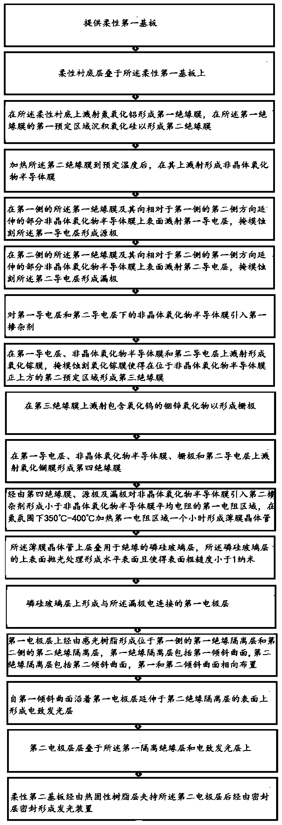
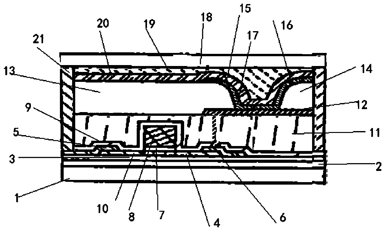
[0042] For better understanding, figure 1 It is a schematic diagram of steps of a method for preparing a light-emitting device according to an embodiment of the present invention, such as figure 1 As shown, a method for preparing a light-emitting device includes the following steps:

[0043] providing a flexible first substrate 1,

[0044] A flexible substrate 2 is stacked on the flexible first substrate 1,

[0045]Aluminum oxynitride is sputtered on the flexible substrate 2 to form a first insulating film 3, silicon oxide is deposited on a first predetermined region of the first insulating film 3 to form a second insulating film, and silicon oxide is formed into a second insulating film. Oxygen can be supplied to the amorphous oxide semiconductor film 4 during filming, and oxygen vacancies in the film can be filled to improve characteristics.

[0046] After heating the second insulating film to a predetermined temperature, an amorphous oxide semiconductor film 4 is formed ...


PUM

PropertyMeasurementUnit
Surface roughnessaaaaaaaaaa
Average surface roughnessaaaaaaaaaa

Abstract

The invention discloses a preparation method of a light-emitting device and the light-emitting device. The preparation method comprises: heating a second insulating film to a preset temperature; sputtering and forming an amorphous oxide semiconductor film on the second insulating film; sputtering on a first conductive layer, the amorphous oxide semiconductor film and a second conductive layer to form a gallium oxide film; carrying out masking etching on the gallium oxide film so that a third insulating film is formed in a second predetermined region directly above the amorphous oxide semiconductor film; introducing a second dopant into the amorphous oxide semiconductor film via the fourth insulating film, the source electrode and the drain electrode to form a first resistance region smaller than the average resistance of the amorphous oxide semiconductor film; forming a first insulation isolation layer located on the first side and a second insulation isolation layer located on the second side opposite to the first side on the first electrode layer through photosensitive resin, oppositely arranging the first inclined curved surface and the second inclined curved surface, and forming an electroluminescent layer on the surface of the second insulation isolation layer by extending from the first inclined curved surface along the first electrode layer.

Description

technical field [0001] The invention relates to the technical field of electroluminescence, in particular to a method for preparing a light emitting device and the light emitting device. Background technique [0002] Flexible thin film transistors are widely used in, for example, electroluminescent display devices. In order to obtain a more powerful display device, flexible thin film transistors with higher electrical characteristics are required, but the existing flexible thin film transistors often have the problem of low field effect mobility, which limits the high electrical characteristics. The electrical characteristics are improved by increasing the drive and high-speed response signals, which brings disadvantages such as increased cost and the need for additional components, and the improvement range of the electrical characteristics is also extremely limited. [0003] The above information disclosed in this Background section is only for enhancement of understandin...

Claims


Application Information

Patent Timeline
IPC IPC(8): H01L27/12H01L21/77H01L27/32G02F1/1368
CPCH01L27/1225H01L27/1218H01L27/1248H01L27/1259G02F1/1368H10K59/12
Inventor 不公告发明人
Owner ANHUI HUITENG INTELLIGENT TRANSPORTATION TECH CO LTD
Features
  • R&D
  • Intellectual Property
  • Life Sciences
  • Materials
  • Tech Scout
  • Unparalleled Data Quality
  • Higher Quality Content
  • 60% Fewer Hallucinations
Learn More