Schottky back gate metal oxide semiconductor field effect phototransistor with sunlight blind area

A technology of oxide semiconductors and phototransistors, applied in semiconductor devices, circuits, electrical components, etc., can solve the problems of device performance degradation, low thermal conductivity, large dark current, etc., to reduce power loss, increase operating frequency, strengthen The effect of control

Pending Publication Date: 2020-08-11
XIDIAN UNIV
View PDF9 Cites 3 Cited by
  • Summary
  • Abstract
  • Description
  • Claims
  • Application Information

AI Technical Summary

Problems solved by technology

Although using Ga 2 o 3 Thin films have the advantages of small volume, less defects, and cost savings, but usually this structure has the disadvantages of large dark current and long recovery process as a photodetector, and because Ga 2 o 3 The thermal conductivity of the material itself is low, resulting in excessive temperature in practical applications, resulting in a decrease in device performance

Method used


Image

  • Schottky back gate metal oxide semiconductor field effect phototransistor with sunlight blind area
  • Schottky back gate metal oxide semiconductor field effect phototransistor with sunlight blind area
  • Schottky back gate metal oxide semiconductor field effect phototransistor with sunlight blind area

Examples


Embodiment 1

[0034] Embodiment 1: prepare Ga 2 o 3 Schottky contact back gate MOSFET with a film thickness of 100nm.

[0035] Step 1, transfer Ga 2 o 3 The thin film forms the channel layer.

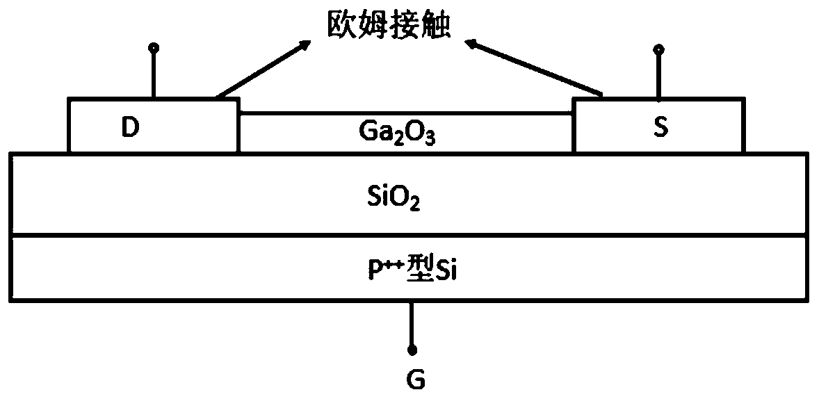
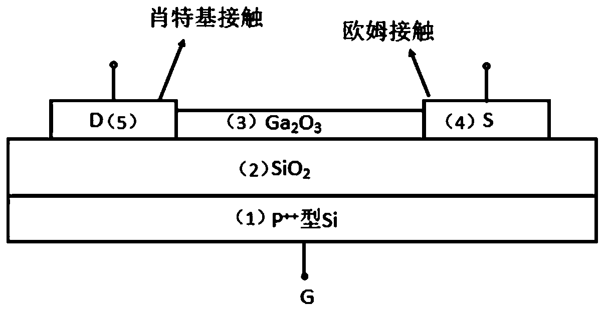
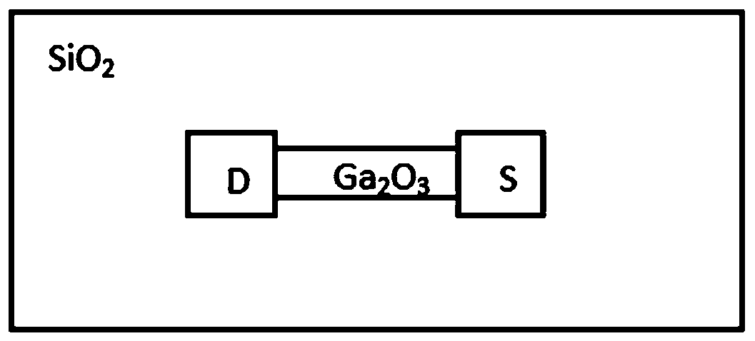
[0036] 1.1) Select the back gate oxide substrate, the two sides of which are P++ type Si and SiO respectively 2 Oxide dielectric layer, in which P++ type Si is used as the back gate, with a thickness of 650nm, SiO 2 As a substrate, the thickness is 200nm, such as Figure 4 as shown in (a);

[0037] 1.2) Ga 2 o 3 The material is peeled onto the blue glue along the 100 crystal direction, and the Ga is reduced by repeated tearing 2 o 3 The thickness of Ga 2 o 3 Thin films were transferred onto the above substrates, such as Figure 4 (b);

[0038] 1.3) After the transfer is successful, place the transferred sample in acetone, absolute ethanol, and deionized water for 10 minutes, and then dry it with a nitrogen gun. The ultrasonic cleaning power should be adjusted to ensure that Ga 2 o 3 T...

Embodiment 2

[0052] Embodiment 2: preparation of Ga 2 o 3 Schottky contact back gate MOSFET with a film thickness of 200nm.

[0053] Step 1, transfer Ga 2 o 3 The thin film forms the conductive layer.

[0054] 1a) Select the back gate oxide substrate, the two sides of which are P++ type Si and SiO respectively 2 Oxide dielectric layer, in which P++ type Si is used as the back gate, with a thickness of 800nm, SiO 2 As a substrate, the thickness is 250nm, such as Figure 4 (a);

[0055] 1b) Ga 2 o 3 The material is peeled onto the blue glue along the 100 crystal direction, and the Ga is reduced by repeated tearing 2 o 3 The thickness of Ga 2 o 3 Thin films were transferred onto the above substrates, such as Figure 4 as shown in (b);

[0056] 1c) After the transfer is successful, place the transferred sample in acetone, absolute ethanol, and deionized water for 10 minutes, and then dry it with a nitrogen gun. The ultrasonic cleaning power should be adjusted to ensure that Ga 2...

Embodiment 3

[0070] Embodiment 3: prepare Ga 2 o 3 Schottky contact back gate MOSFET with a film thickness of 300nm.

[0071] Step A, transfer Ga 2 o 3 thin film forming conductive layer

[0072] A1) Select the back gate oxide substrate, the two sides of which are N++ type Si and SiO respectively 2 Oxide dielectric layer, in which N++ type Si is used as the back gate, with a thickness of 500nm, SiO 2 As a substrate, the thickness is 300nm, such as Figure 4 as shown in (a);

[0073] A2) Ga 2 o 3 The material is peeled onto the blue glue along the 100 crystal direction, and the Ga is reduced by repeated tearing 2 o 3 The thickness of Ga 2 o 3 Thin films were transferred onto the above substrates, such as Figure 4 as shown in (b);

[0074] A3) Adjust the ultrasonic cleaning power, and place the transferred sample in acetone, absolute ethanol, and deionized water for 10 minutes in order to ensure that Ga 2 o 3If the film does not come off, blow it dry with a nitrogen gun.

...


PUM

PropertyMeasurementUnit
Thicknessaaaaaaaaaa
Thicknessaaaaaaaaaa
Thicknessaaaaaaaaaa

Abstract

The invention discloses a Schottky back gate metal oxide semiconductor field effect phototransistor based on a transfer printing gallium oxide thin film. The phototransistor comprises a polysilicon gate (1), a SiO2 dielectric layer (2), a Ga2O3 film channel layer (3), a source electrode (4) and a drain electrode (5). The Ga2O3 film channel layer (3) is printed between the source electrode (4) andthe drain electrode (5) on the SiO2 dielectric layer (2), the source electrode (4) adopts ohmic contact, the drain electrode (5) adopts Schottky contact, and a Schottky back gate composite structure is formed. According to the invention, the two advantages of the unidirectional conductive characteristic and the grid controllability of the Schottky diode are combined, the control capability of thedevice is improved, the reverse leakage current is reduced, the light-dark current ratio is increased, the reliability of the device is enhanced, and the phtototransistor can be used for flame detection, secret space communication, target early warning and tracking and solar blind imaging.

Description

technical field [0001] The invention belongs to the technical field of semiconductor devices, in particular to a schottky-contact back-gate metal oxide semiconductor field-effect photoelectric crystal MOSFEPT, which can be used for flame detection, secure space communication, target early warning and tracking, and solar blind imaging. [0002] technical background [0003] gallium oxide Ga 2 o 3 Semiconductor materials have a long history. As early as the 1950s, the polycrystalline gallium oxide and its stable regions were first reported. However, gallium oxide was not paid attention to at that time due to the limitation of technology at that time. In recent years, with the development of science and technology, people have discovered the potential advantages of gallium oxide in the fields of photodetectors and electronic power devices, and more and more related researches have been conducted. According to the statistics of relevant personnel, since the 1950s, the number o...

Claims


Application Information

Patent Timeline
IPC IPC(8): H01L31/113H01L31/0224H01L31/18
CPCH01L31/1136H01L31/022408H01L31/18Y02P70/50
Inventor 张春福成亚楠陈大正冯倩张进成郝跃
Owner XIDIAN UNIV
Why Eureka
Try Eureka